
-
-
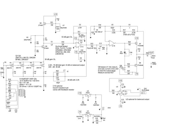
Building your Pearl 3 phonostage.
-
Things to do -
-
1) Download and PRINT the .pdf in this link - https://www.diyaudio.com/community/threa...
-
2) Want the chassis shown in the guide? Order here - https://modushop.biz/site/index.php?rout...
-
-
-
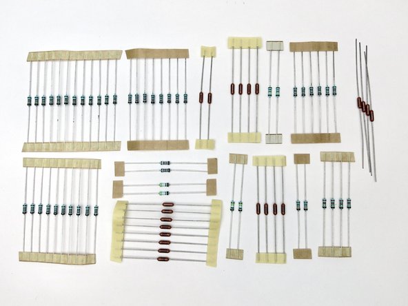
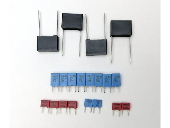
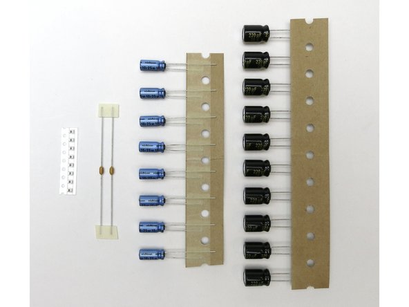
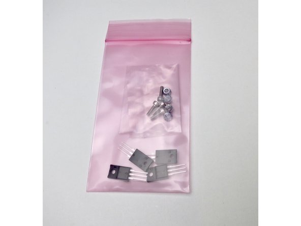
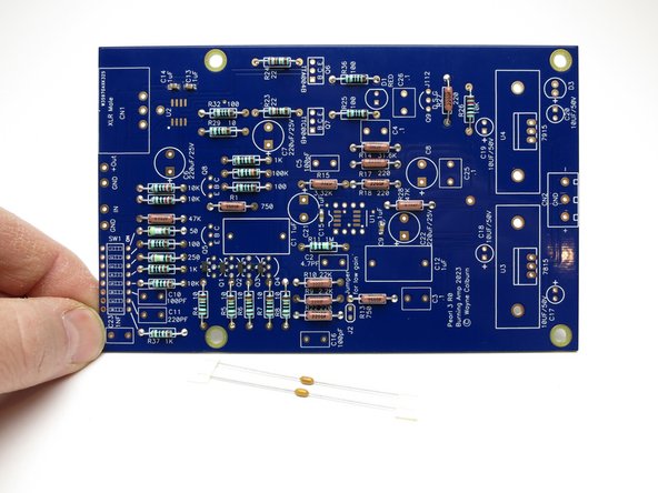
These photos show the contents of the Pearl 3 “pioneer” kit from winter 2023/24.
-
All components to stuff the RIAA PCBs are included.
-
Photo 2 - Pearl 3 RIAA boards.
-
Photo 3 - PSU board.
-
-
-
The build document is a PDF that can be found in Post #1 of the Pearl 3 builder's thread on DIYAudio.com Print the document. Read through this a few times before building. This is a complex project.
-
Print the schematic separately or use the version in the build guide. Mark the components as you put them onto the PCBs. This is a way to double-check the values as you confirm the component values and populate the boards.
-
-
-
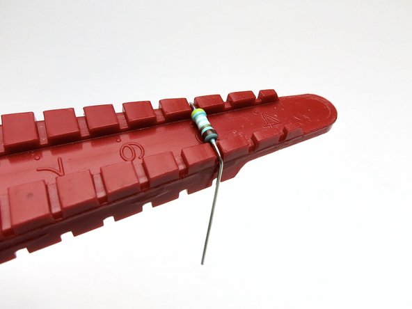
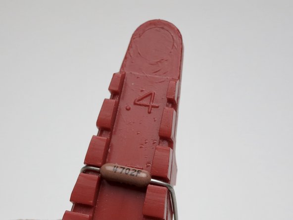
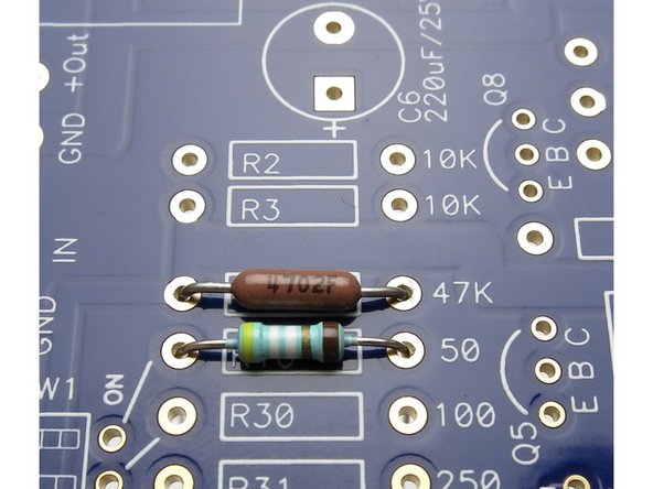
As you can see, there are a lot of resistors, and many values.
-
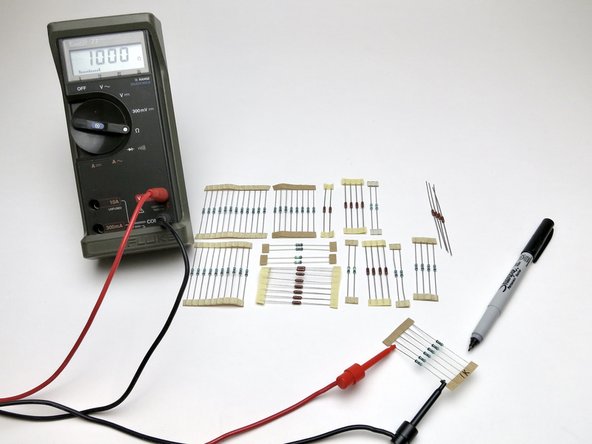
Photo 2 - Measure and label everything. Measure EVERY RESISTOR before placing in the board
-
-
-
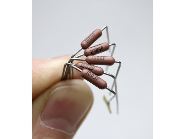
The Dale RN/CMF series are 3-digit + multiplier.
-
The bottom, marked "1003" is 100K, since you have 100 and three zeroes. The one marked "1002" is 10K.
-
"1500" is 150 ohm, as the value is 150 plus zero zeroes. This is not 1.5K
-
Below 100 ohm the letter "R" is placed at the decimal place, "27R4" is 27.4 ohms, and "10R0" os 10 ohms.
-
Banded resistors follow the 5-band standard code.
-
But even with that easy system, Measure All Resistors before stuffing and soldering.
-
Note - This is a generic photo, this project may not have the values shown.
-
-
-
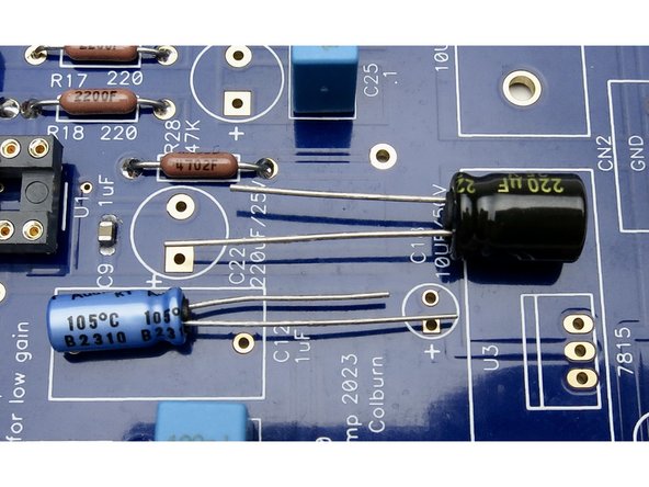
Photo 1 - Top 1uF. Middle 0.1uF. Bottom 100pF, 1nF, 220pF
-
Photo 2, L to R, 1uF SMD, 4.7pF, 10uF, 220uF
-
-
-
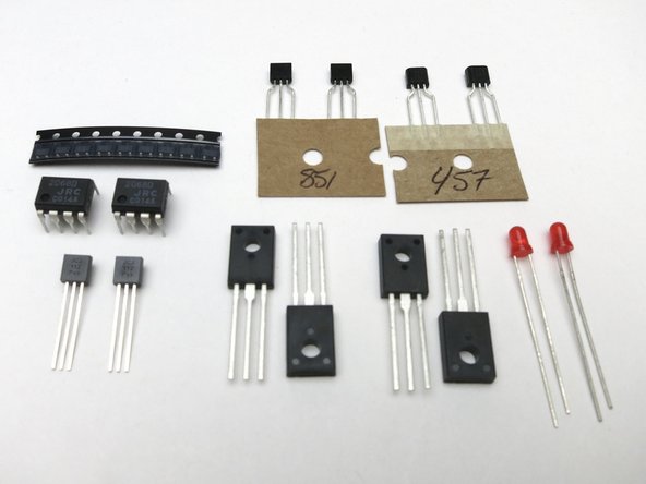
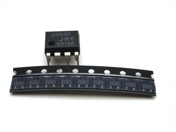
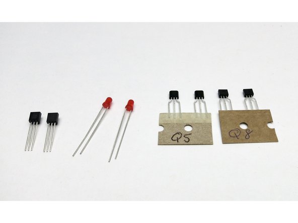
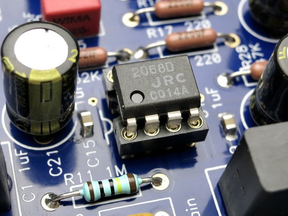
The Transistors, opamp, and reference LEDs are packaged together.
-
We will go over them individually in the next few slides.
-
-
-
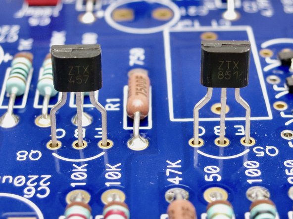
Please note that the LED in the transistor bag are precision voltage references, that happen to light up. Do not substitute any other color. Replace only with Lite-On LTL-1CHE.
-
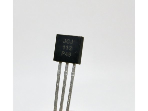
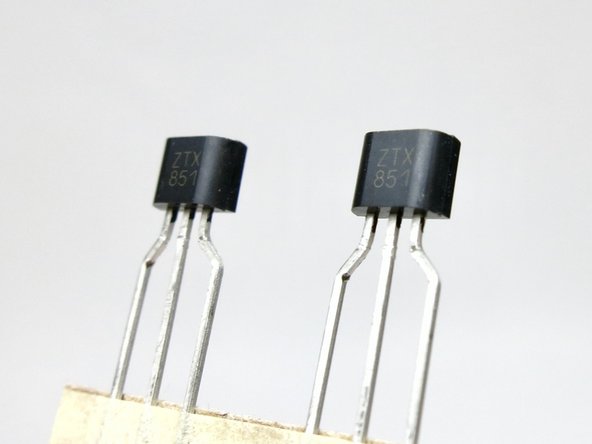
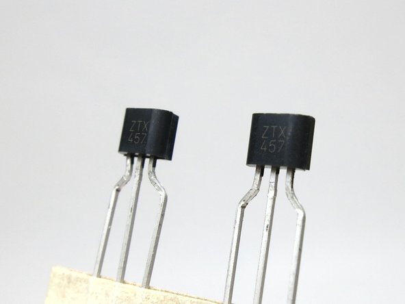
J112 are loose and have straight leads.
-
ZTX851 and ZTX457 may be loose, or on tape and labeled. Leads may be straight or bent.
-
-
-
Photo 1 - J112
-
Photo 2 - ZTX851. For Q5.
-
Photo 3 ZTX457. For Q8.
-
-
-
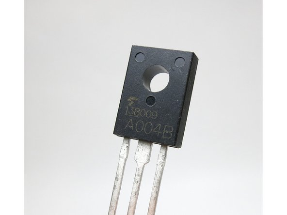
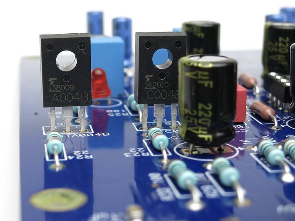
Photo 1 - TTA004b. P-channel
-
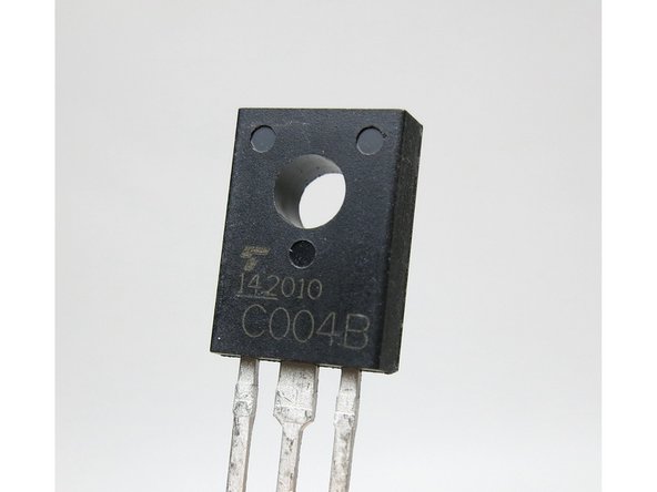
Photo 2 - TTC004b. NPN
-
-
-
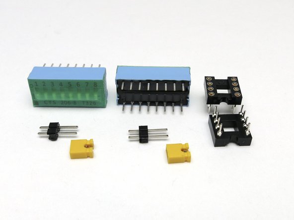
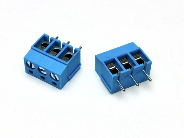
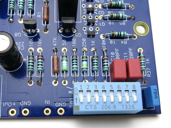
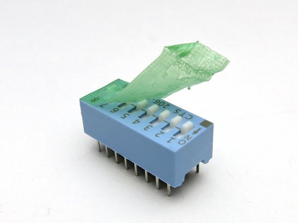
DIP switches, DIP sockets, and the header pins with jumpers.
-
-
-
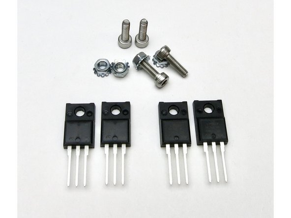
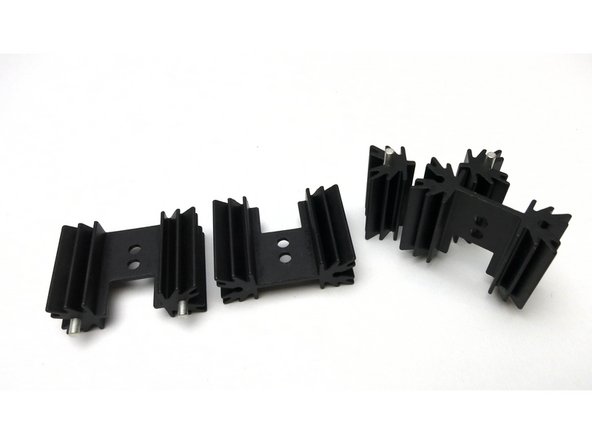
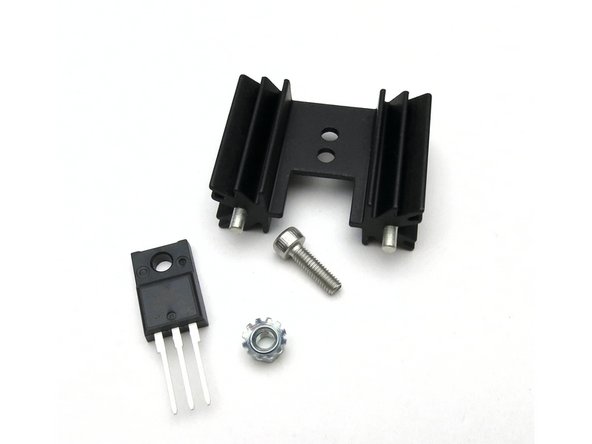
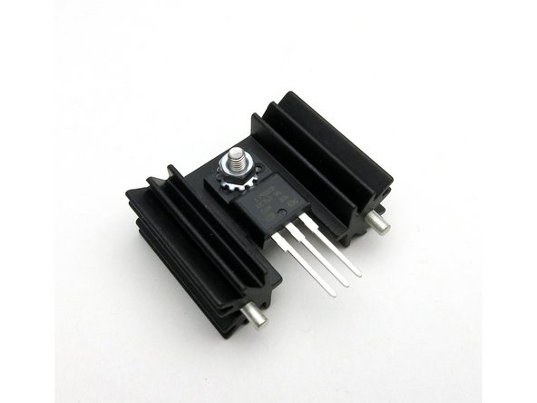
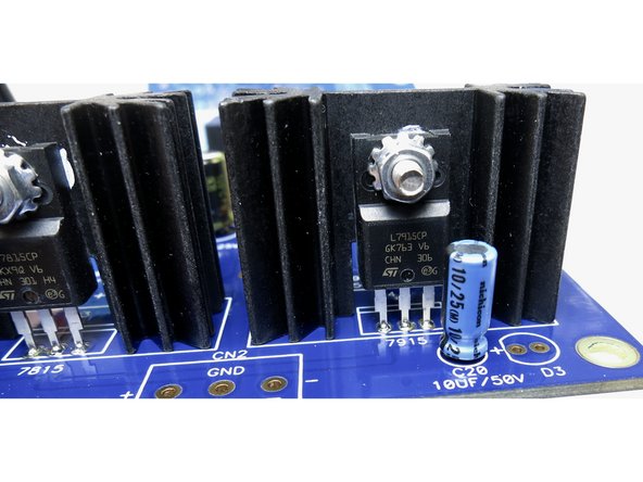
7815 and 7915 regulators, and mounting hardware.
-
Photo 2 - PC mount heatsinks.
-
-
-
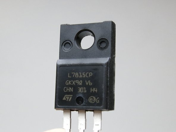
Photo 1 - 7815 Regulator for V+.
-
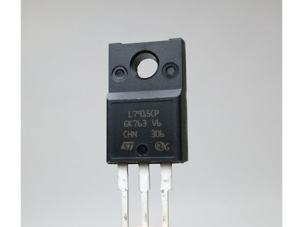
Photo 2 - 7915. The V- regulator.
-
-
-
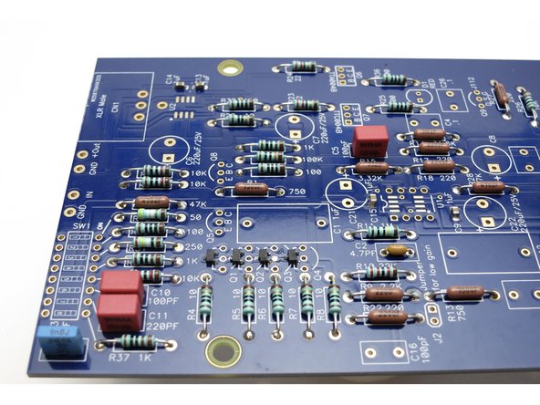
Print this out for reference when building. Check off components as you measure and stuff them into the board.
-
If you're interested in adjusting the gain settings for your build, please refer to the build document for the calculations.
-
-
-
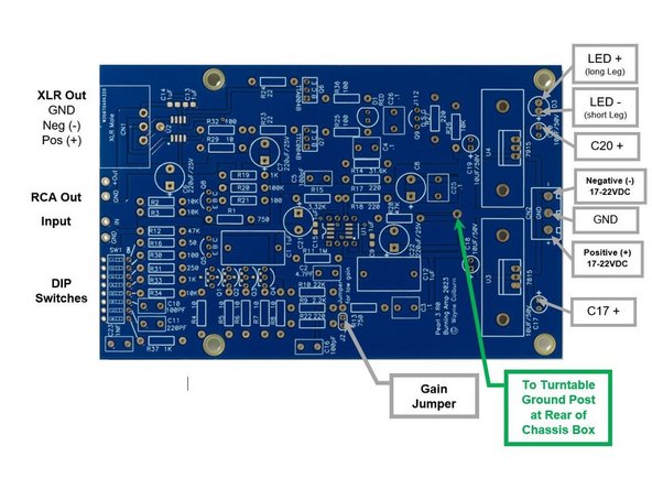
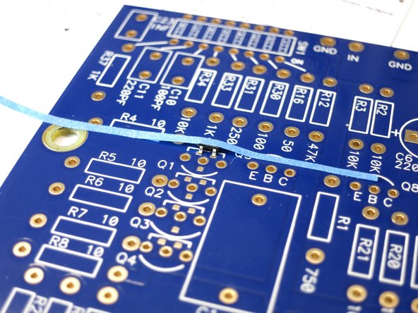
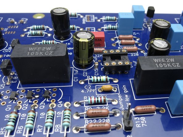
Photo 1 - See notes highlighting key points on the Pearl 3 PCB
-
-
-
If this is your first time working with SMD components, consider buying a SMD practice kit on Amazon or similar. You will want tweezers and a magnifying glass or magnifying visor to see the components clearly.
-
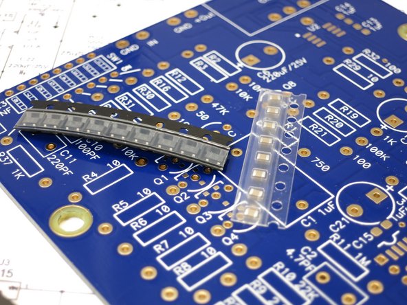
Solder the capacitors, the SMD JFETs (if using SMDs), op amps (if using SMD op amp fixed to PCB), and the optional balanced line driver chip. See Photo 3 for an example of using tape to hold SMD device in place for soldering.
-
Test connections from component legs to next point on PCB/Schematic to confirm proper connections. Set DMM to Ohms or continuity buzzer. Example C9 to ground and to -15V or C22 negative connection. Check off connections on schematic. Fix any problems NOW before moving on to through hole components.
-
-
-
Testing JFET soldering.
-
This must be done before you stuff anything else.
-
-
-
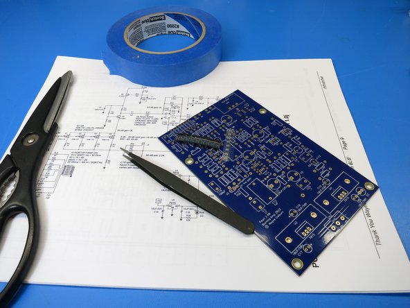
A short video showing soldering of the SMD capacitors
-
-
-
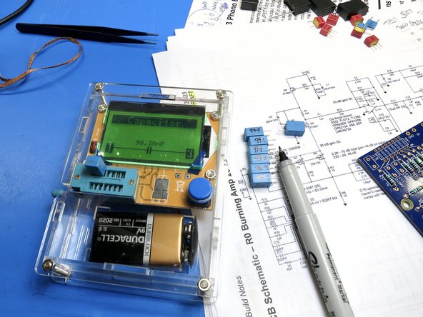
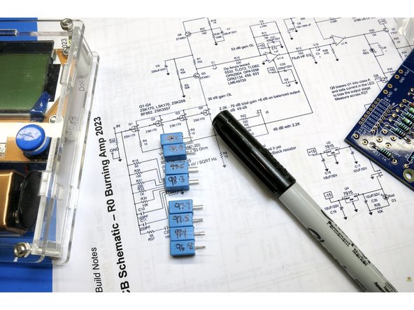
OPTIONAL - This is a Mega328 tester, available on Amazon or eBay for $15-20. It’s a universal electronics tester, place a component into the Mega328 and it will determine what it is, and measure, as well as show pins if it’s a semiconductor. Neat!
-
Measure your caps and grab the two closest pairs - these matched pairs will go into the same positions L and R, for channel matching the RIAA filter caps. Pair one L/R C3. Pair two L/R C4
-
The rest of the 0.1 caps do not benefit at all to being matched, as they are not filter caps. C25 is a film bypass around an electrolytic and not even necessary, and C26 is part of the bias spreader in the output stage.
-
-
-
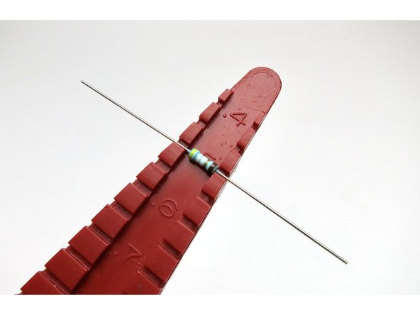
Lead bend tool. 0.5"
-
Photo 2 - Striped resistors
-
Photo 3 - Numerical resistors, bend leads with the value facing up. The value is 4 digits and has a "F" in the last place.
-
Neatness counts. If you don't have a lead bender tool, get one. They are wonderful and you’ll use it in every project after. :)
-
-
-
0.5" bends will fit all resistors.
-
Photo 2 - Striped resistors, thick brown band to the right. The thick brown is the 5th digit, I.E., in this orientation they read L to R.
-
Numerical resistors, value facing up, aligned with the F to the right.
-
Neatness counts. Make it look good.
-
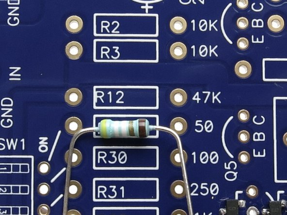
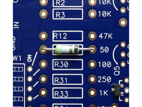
Insert resistors according to schematic and PCB. Don't forget to measure resistor values! Measure twice, solder once!
-
Bend resistor leads on the bottom of the PCB to hold them in place.
-
Solder resistors.
-
-
-
Although it looks somewhat like a resistor, you’ll find the 4.7pF capacitor in the capacitor bag.
-
Bend legs for C2 (4.7pF) capacitor and insert into PCB
-
-
-
Insert film capacitors and solder.
-
-
-
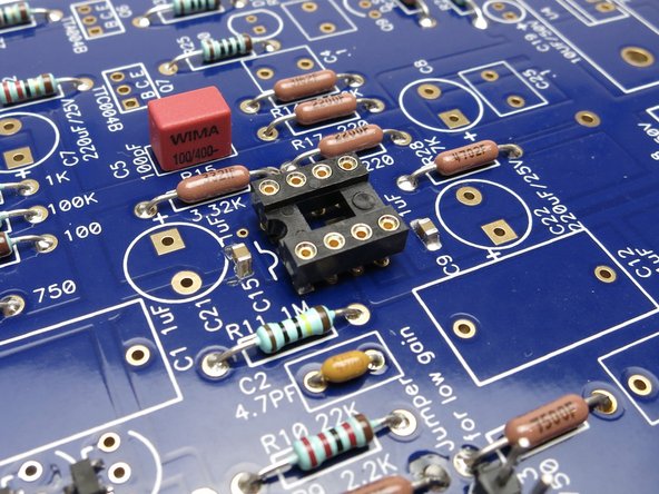
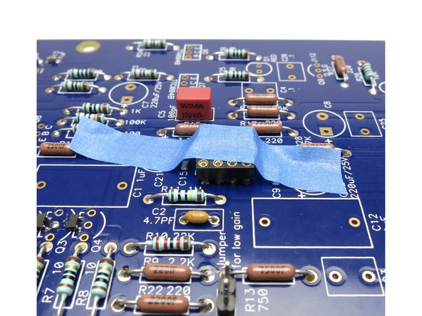
If using DIP op amps, insert the DIP socket as shown in Photo 1. NOTE the "notch" shown on the PCB and on the socket.
-
Use tape to hold socket in place, then solder the DIP socket. See Photo 2
-
Skip this step if using SMD op amps soldered directly to the PCB. Of course, you could get SMD to DIP adaptors if you want to roll opamps, in which case install the socket.
-
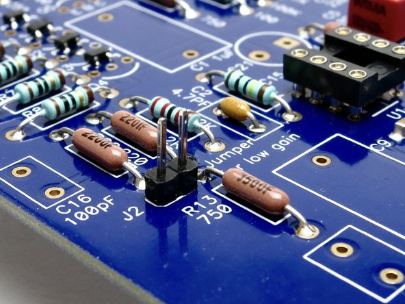
Install the jumper the same way. Tape it in place, flip the PCB and solder.
-
-
-
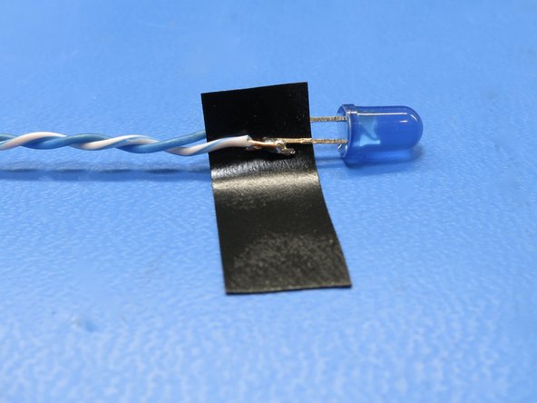
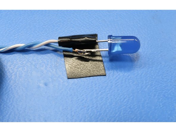
Cut positive LED lead (longer lead / Anode) and solder wire to PCB. Note which color is positive!
-
Repeat procedure for negative lead ( shorter lead / Cathode)
-
Insert electrical tape to keep leads separated and covered.
-
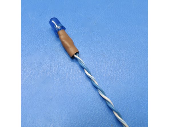
Add heatshrink.
-
-
-
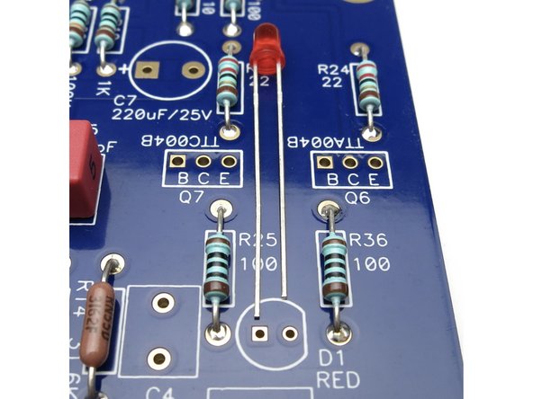
LED long leg (positive) in square hole. Cathode (negative) is short leg, and the flat on the silk.
-
Electrolytic capacitor long leg (positive) to square hole. The schematic indicates 50V capacitors in some locations. 25V are perfectly sufficient.
-
DIP socket notch lines up as shown on silkscreen. Pin 1 of the op amp is designated by the dot.
-
-
-
Stuff and solder the remaining semiconductors.
-
Confirm each semiconductor against the build document and the "Transistor Identification" steps above.
-
-
-
Orient as shown. Move switch towards resistors/caps to turn ON.
-
Photo 2 - Note the green tape is shipping protection, remove before use.
-
-
-
Mount regulators to heatsinks with screw and kepnut. See Photo 2.
-
Mount heatsinks and regulators into PCB. PAY ATTENTION to 7815 (Positive) and 7915 (Negative) markings on PCB and regulators.
-
Solder regulators and heatsink legs to PCB. Heatsink legs will require additional patience and/or a higher heat setting on your solder station.
-
-
-
Order of operations -
-
1) Attach regulator to heatsink, with nut+ screw, tighten only a little.
-
2) Insert assembly into PCB.
-
3) Solder heatsink posts as shown in this video.
-
4) Tighten screw. (not too tight... it's plastic... but enough to ensure there is good contact between the heatsink and regulator.)
-
5) Solder regulator pins.
-
-
-
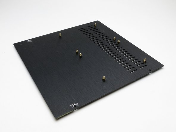
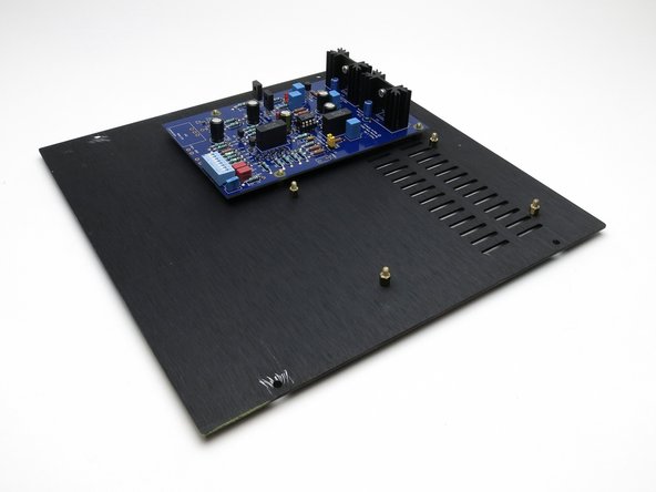
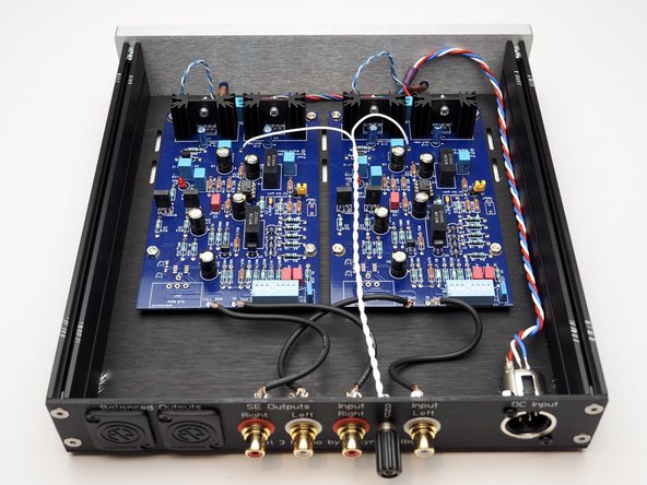
Purchase M3x5 standoffs and attach as shown. The vent holes are at the front of the chassis.
-
Mount PCBs to standoffs.
-
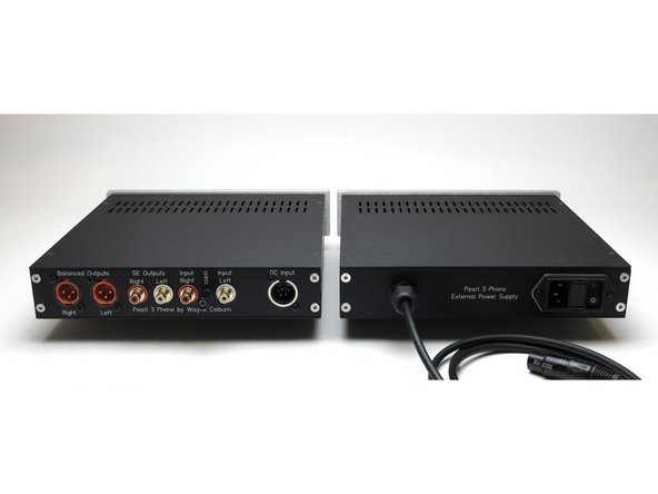
Now it's time to wire it up!
-
-
-
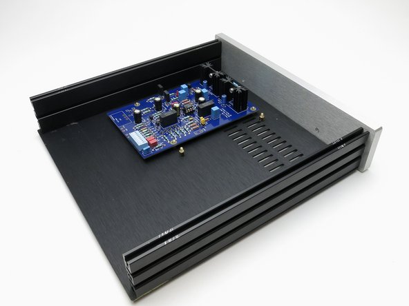
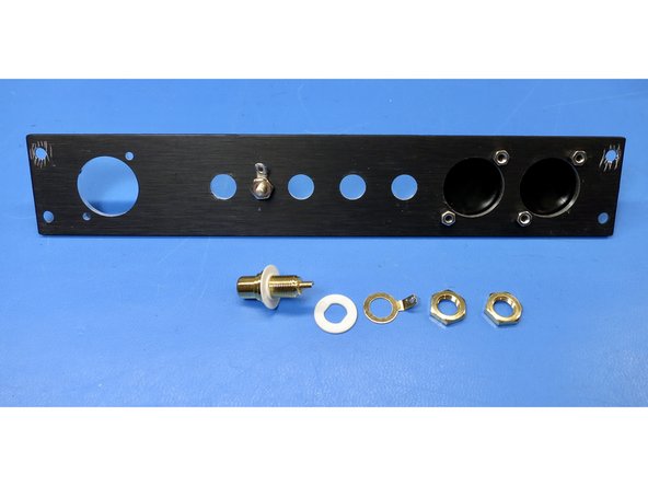
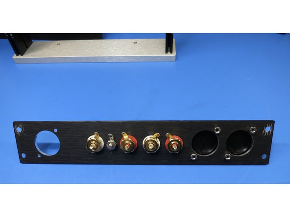
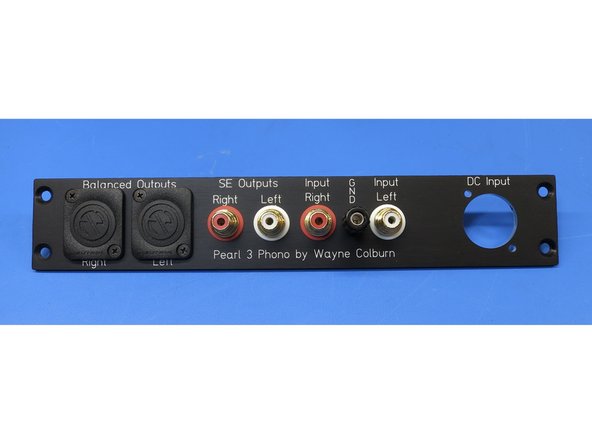
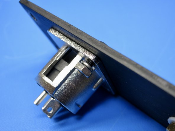
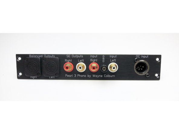
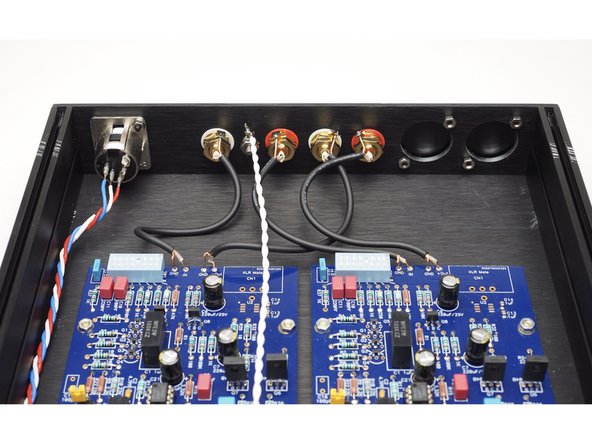
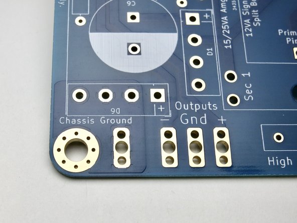
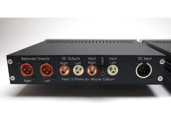
Attach jacks and post as shown. make sure the RCA insulators are used and they do not touch the metal of the chassis.
-
The ground post must touch chassis and it’s very helpful to scrape the anodization off the panel to ensure it touches bare aluminum.
-
XLR output are optional, Neutrik blanking plates are shown.
-
-
-
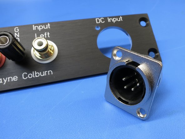
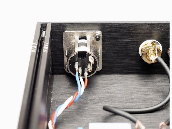
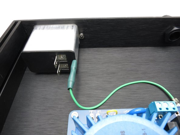
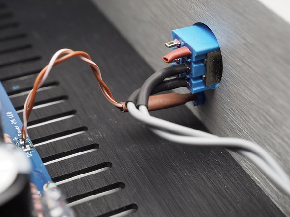
4-pin XLR is used for the DC power umbilical.
-
-
-
Insert wisdom here.
-
-
-
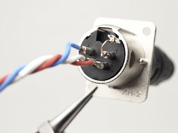
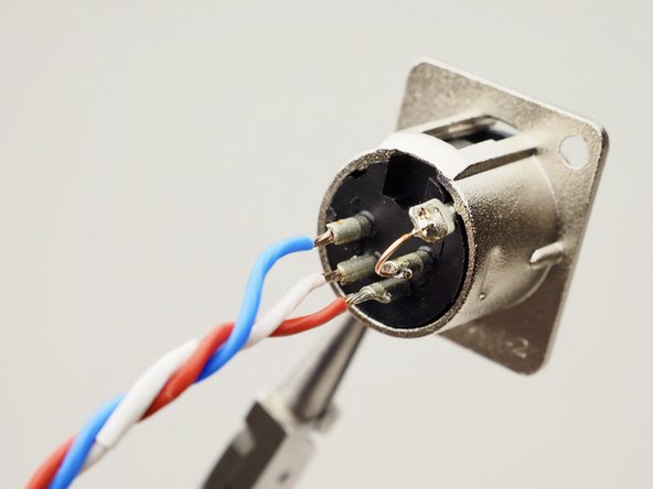
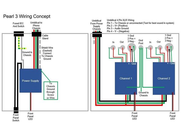
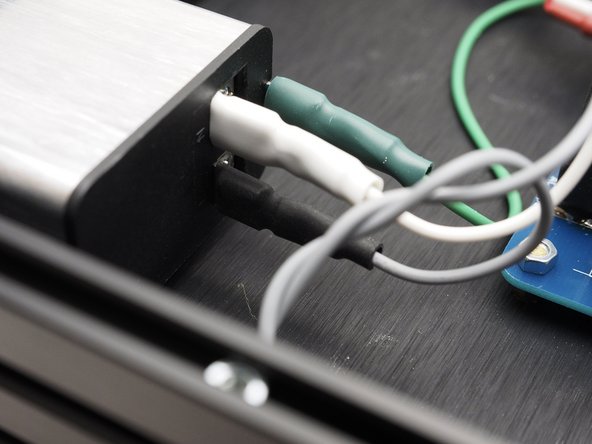
Power umbilical and jack should be wired as shown -
-
Pin 1 Shield Note that pin 1 is connected to the jack tab.
-
Pin 2 V+
-
Pin 3 GND
-
Pin 4 V-
-
-
-
Very straightforward and logical.
-
Signal wiring in this example is Mogami W2330, of course you could use whatever you like.
-
Power wiring is just 3 strands twisted together.
-
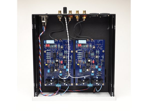
CHASSIS PANEL CONNECTION - in this photo it’s evident that there are many scratches on the various chassis panels. This is because all 6 panels need to be electrically conductive to one another. The anodizing and/or paint must be removed to bare metal to ensure the panels are all connected.
-
Failure to do this can lead to hum, which can only be fixed by getting these panels connected. :)
-
-
-
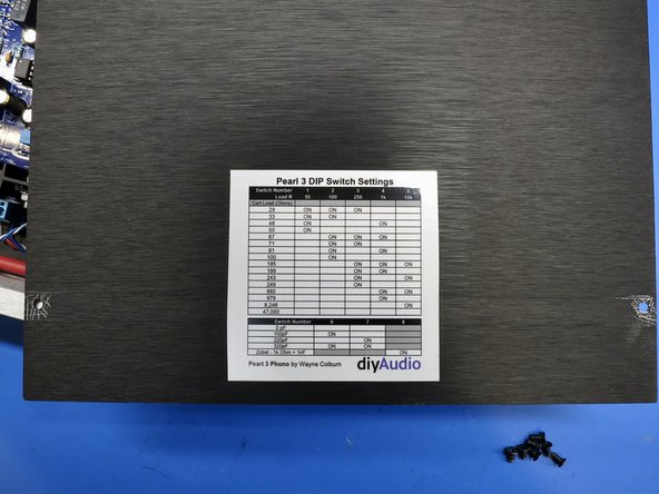
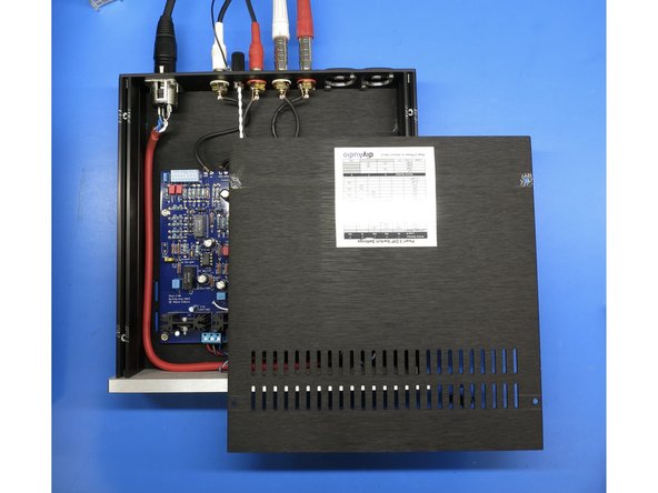
Place sticker on inside of the top panel.
-
When you open the lid to change loading, it will be in a convienent location for reference. :)
-
-
-
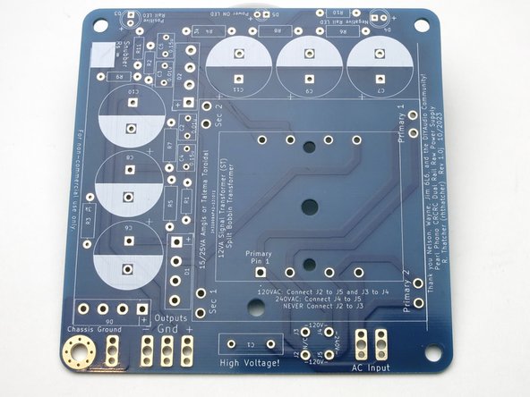
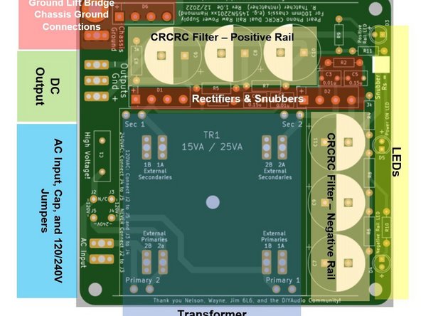
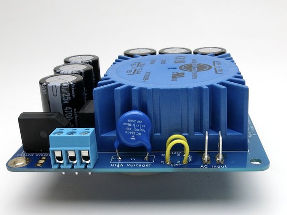
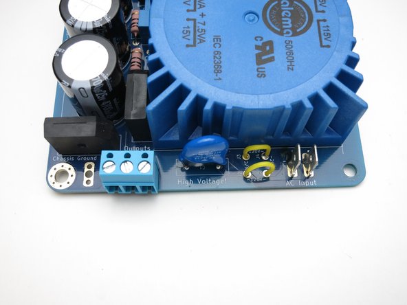
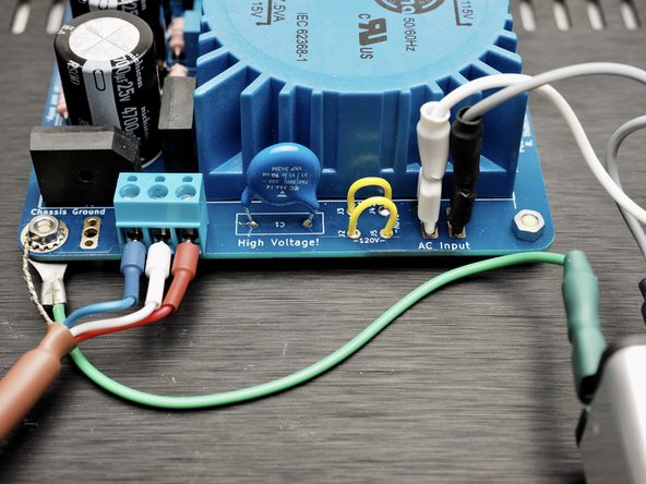
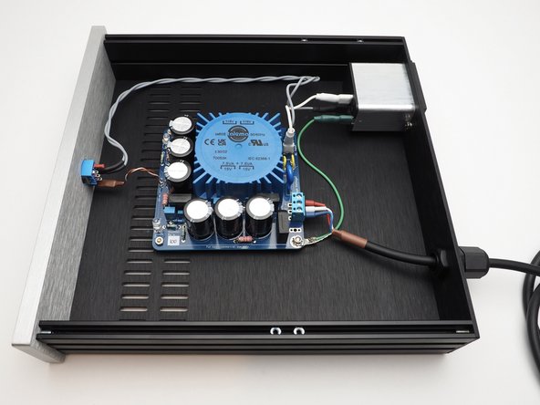
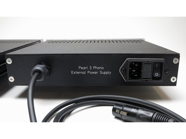
Photo 1 shows the CRCRC power supply PCB.
-
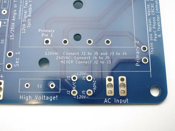
Photo 2 shows the AC input and AC 120/240VAC Jumper positions.
-
Photo 3 shows the Chassis Ground connection points and DC output where the umbilical cable will connect. Chassis ground is connected to the audio ground by D6 ground breaker diode bridge. Chassis needs connected to the Chassis Ground on the PCB either through the screw or the solder pad next to the screw.
-
-
-
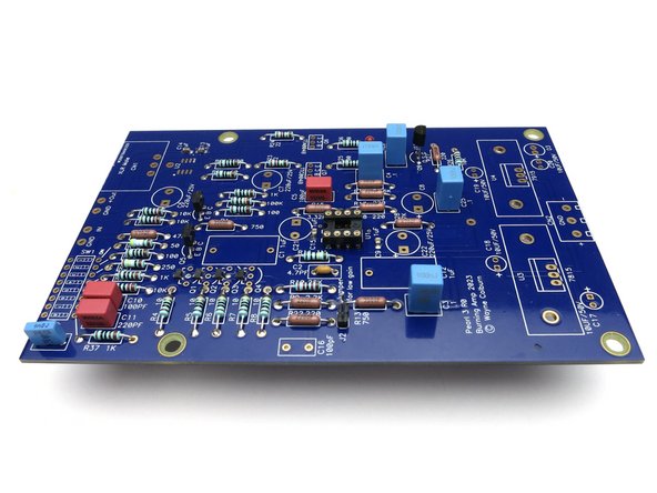
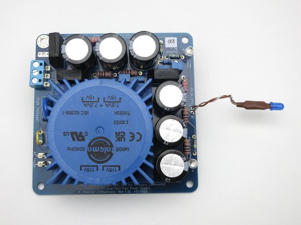
Power Supply PCB breakdown.
-
-
-
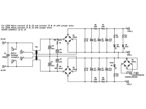
Print this power supply schematic for reference when stuffing parts.
-
-
-
Wiring concept diagram
-
-
-
For 120V Mains connect J2 & J5 and connect J3 & J4 with jumper wires (e.g. old resistor leads)
-
For 240V Mains connect J4 & J5 with jumper wires
-
NEVER CONNECT J2 & J3
-
Photos 1 & 2 show jumpers with yellow insulation configured for 120VAC.
-
Populate and solder the PCB in the same order as the Phono PCBs. Lowest items first - resistors, LEDs, jumpers, then caps/bridges, and finally the transformer.
-
-
-
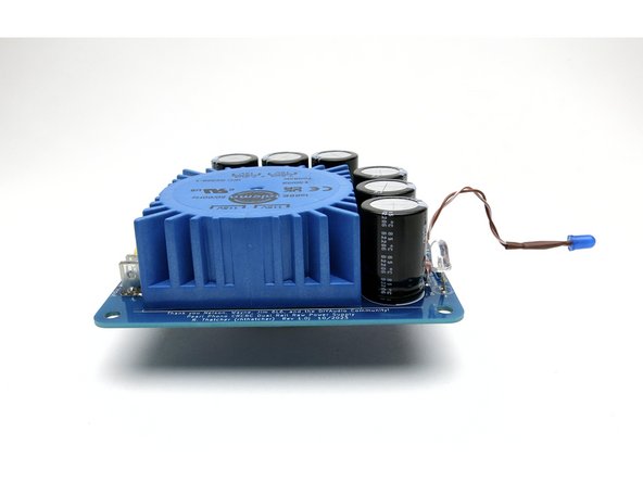
Prepare the power supply front panel indicator LED similar to the phono stage LEDs.
-
-
-
Connect an earth ground wire (Preferred color: Green or Green/Yellow) from IEC ground connection to chassis. This can be direct to a hole in the chassis or to the power supply "Chassis ground" points on the power supply PCB. Be sure to scrape away paint or anodization to expose bare chassis metal, and use a star or split lock washer.
-
Test continuity from the outer IEC ground pin to chassis metal to confirm proper connections. Set your DMM to Ohms or continuity buzzer to test for Zero Ohms or "Buzz"
-
Connect mains wiring according to the build guide diagram. Neutral (white wires in Photos 2&3) from IEC to PCB.
-
Line (grey wires in Photos 2&3) from IEC to switch, switch to PCB "AC Input".
-
Photos show "quick disconnect" spades for AC Line wiring. Optionally, you can use solder connections or terminal blocks for AC Input.
-
-
-
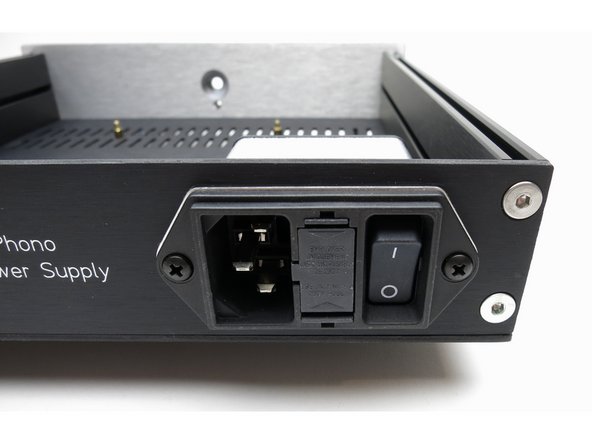
Remember that the switch is connected to live mains AC, use an appropriately rated switch, and insulate properly.
-
It does not have to be a DPDT, I happen to have a bunch of these...
-
-
-
.
-
-
-
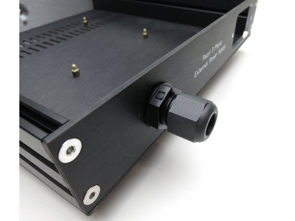
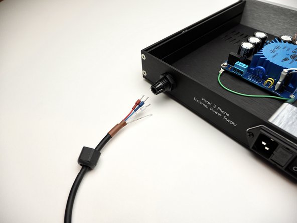
Mount cable gland on rear panel.
-
Thread the umbilical cable through the cable gland leaving the outer connector loose for now.
-
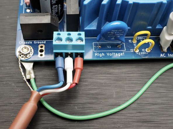
Terminate the umbilical wires to the power supply. Pay attention to align + / GND / - so that they connect correctly from PSU to 4-pin XLR pins/jack and to phono boards.
-
Wire umbilical - Pin 1) Chassis, Pin 2) V+, Pin 3) GND, Pin 4) V-
-
Tighten cable gland to secure the umbilical cable in place.
-
-
-
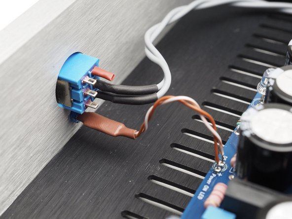
In this diagram, you can see
-
Shield connected to chassis. (pin 1 at plug)
-
V- Blue (pin 4 at plug)
-
GND White (pin 3 at plug)
-
V+ Red (pin 2 at plug)
-
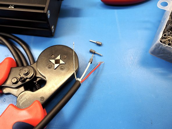
The ferrules are not required, but they are really neat, make a better interface with the terminal, and look great.
-
Umbilical here made from Mogami W2893, of course you can use different, it’s strongly suggested you use a shielded cable with 3+ conductors.
-
-
-
You're almost there, but first it's time to perform some testing.
-
See the TESTING section of the build guide document.
-
Power Wiring check from PSU out to Phono Stage. Power supply power OFF, Umbilical Connected. Measure Resistance from PSU output to each Phono PCB power input connector. Confirm PSU Positive is connected to RIAA Positive. Same for GND and Negative.
-
Next follow the Power Up Tests in the build guide.
-
-
-
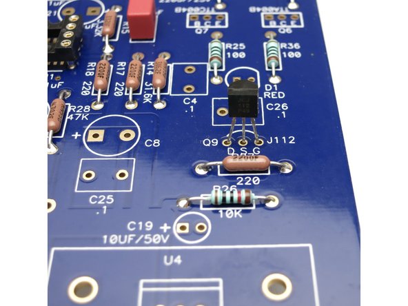
R27 can be tweaked to set the ideal current through the opamp.
-
V=I*R=2mA*220R=0.44V andV=I*R=5mA*220R=1.1V If you measure between 0.44V and 1.1V with R27 = 220R – you’re good to go.
-
Adjustment Example: Measure 2.4V with 220R. Calculated current is 2.4V / 220R = 10.9mA. You can see that current is about 2x the spec, so you need about 2x the resistance to get current down to spec.
-
Is there a 400-500R resistor in the parts bin? Let’s try a 549R, seems pretty close. Measured result is 2.7V. Bias current = 2.7V / 549R = 4.9mA Now it’s in spec! Time to play music!
-
Remember, too much current? Make R bigger. Not enough current? Make R smaller.
-
-
-
Insert wisdom here.
-


Cancel: I did not complete this guide.
6 other people completed this guide.