
-
-
The ACA mini by Nelson Pass.
-
A fantastic amplifier, intended to be used as this boxless PCB, which is a fun industrial look, and saves the major expense of an enclosure.
-
Power is 5W into 8ohm, 8W into 4ohm.
-
This amplifier sounds fantastic, if you have any interest at all, you really should build one. :)
-
-
-
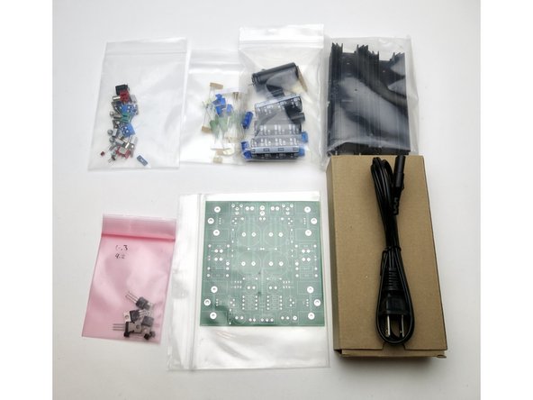
Please read the notes and click through all the photos.
-
Also, download and read Nelson's ACA Mini article
-
Print the schematic and have in front of you when stuffing the PCB
-
Ensure you are using the correct Bill of Materials. The current BOM used in the completion kit is ACA Mini BOM V1.1.
-
-
-
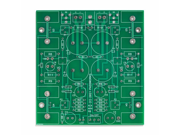
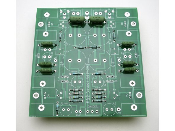
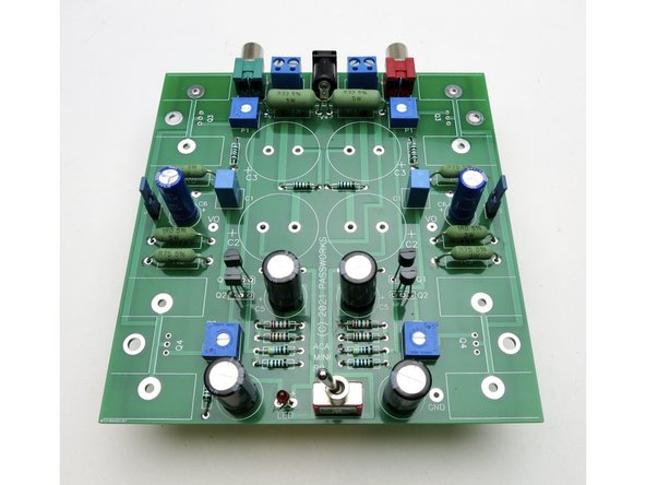
PCB front. All components mount on this side.
-
-
-
This is a beautifully simple kit.
-
PCB
-
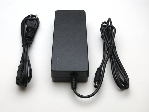
24V 90W PSU brick. Double insulated, Universal input.
-
-
-
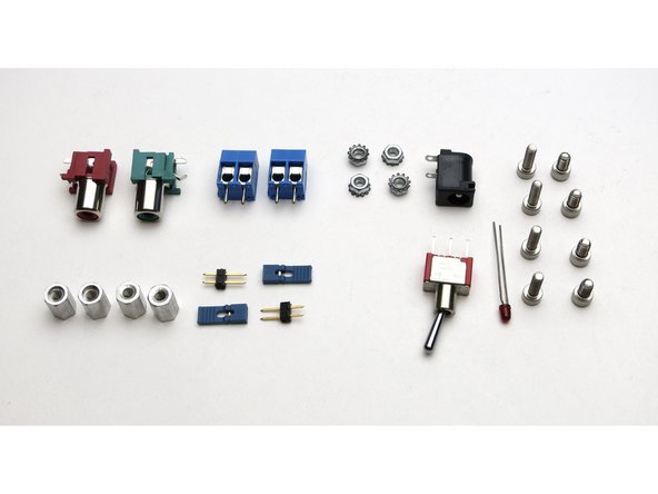
Photo 1 - Connectors and hardware
-
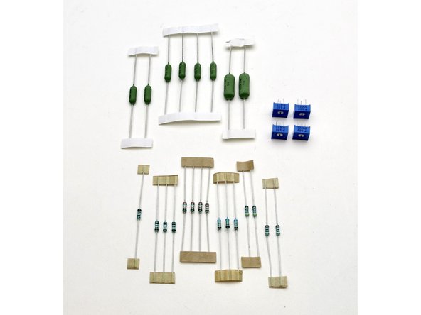
Photo 2 - Rear 15,000uF capacitors. Front 1,000uF (Black cans), 3.3F (blue cans), 1uF film (blue box)
-
Photo 3 - resistors, potentiometers. Please note the pots in the current batch of completion kits require their leads bent before installation, here is how to bend the leads.
-
Neat fact - 3.3F is 3,300,000uF
-
-
-
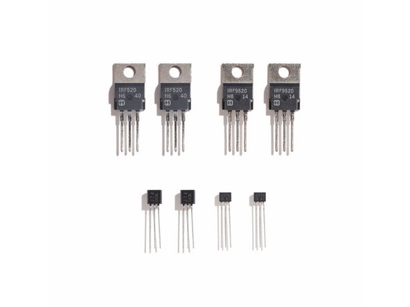
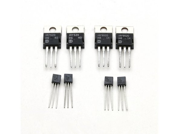
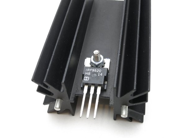
Rear - IRF520 (N-channel Q4) and IRF9520 (P-channel Q3)
-
Small signal Jfets can be LS parts or Toshiba.
-
LSK170, 2SK370, 2SK170 can all be supplied for the N-channel devices intended for position Q1
-
LSJ74, 2SJ74, 2SJ108 can all be supplied for the P-channel devices for use in position Q2
-
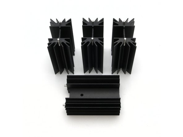
Photo 3 - Heatsinks
-
-
-
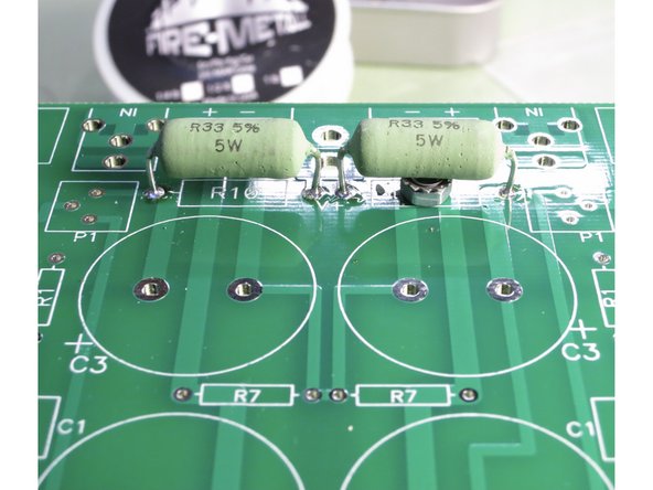
Power resistors are mounted first.
-
Leave some room under them for airflow. The nut is a good gauge.
-
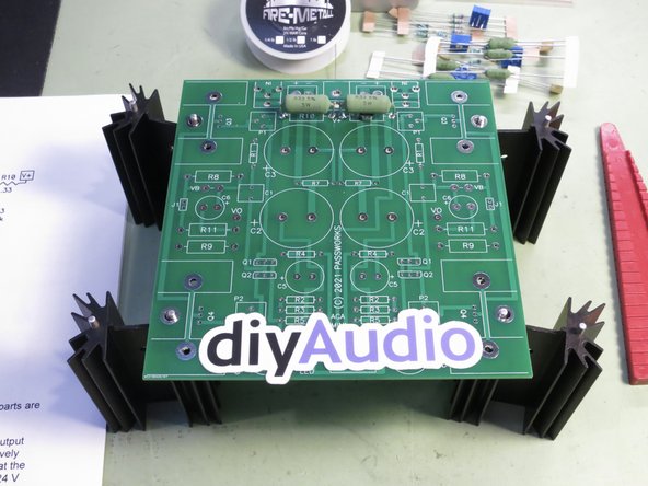
You can use the heatsinks as an impromptu stand for holding the PCB.
-
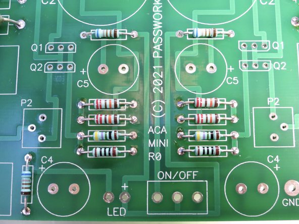
Neatness counts - Bend the leads so the value is readable, and so it reads left to right. The value markings are R33, R75, 1R0.
-
Low-ohmic resistors use "R" as a decimal point. "R33" means 0.33ohm. "1R0" is 1.0ohm.
-
It's difficult to measure low-ohmic resistors because the resistance of your multimeter leads (normally 0.2-0.4Ω) will be added. You can measure your leads and subtract the value, just trust the values which are printed on them, or build a low resistance value test rig.
-
-
-
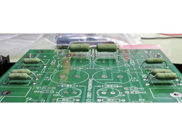
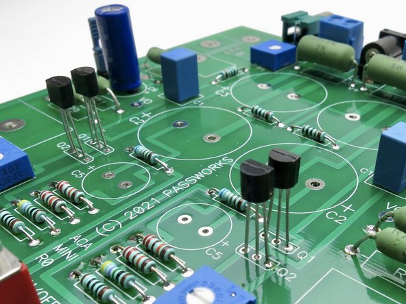
Install and solder the small resistors next.
-
Measure every one before installation.
-
Face them so the heavier brown stripe is on the right. (Or bottom, for the three resistors that point up.)
-
Photo 2 is provided as a reference to help stuffing, but it's much better to measure every one and refer to the schematic before installation.
-
-
-
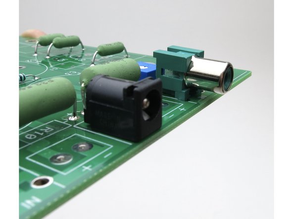
In all cases, make sure the connectors are flat and properly aligned with the PCB before soldering.
-
-
-
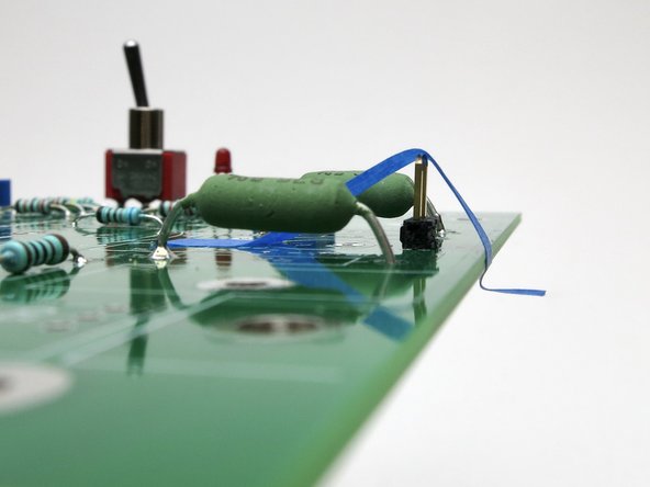
It is very helpful to tape the jumper pins to the PCB before soldering. This will hold them in place and keep the vulgar language down to an absolute minimum.
-
Don't try to hold them on with a finger whilst soldering, that is a fantastic way to burn yourself.
-
-
-
At this point you should have the edge connector items stuffed, and the potentiometers.
-
Power switch orientation does not matter.
-
LED needs to be stuffed with the long lead in the + hole.
-
If you want to swap the LED for a different color, feel free, it's used only to indicate power on/off.
-
-
-
Stuff the small transistors. Watch the orientation, the flat of the device lines up with the flat drawn on the silk.
-
Leave the leads long. I place the PCB on the tabletop, solder one leg from the top to keep it in place, then flip the board and finish the rest of the legs.
-
Small capacitors next. Long lead in the + hole.
-
The - of the capacitor can is marked, but the convention shows the + marked on the silkscreen. So be careful.
-
-
-
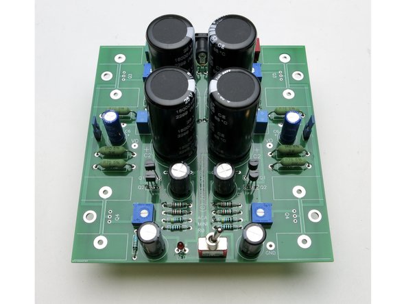
Install the large capacitors. Orient the - marks on the cans all to the inside.
-
-
-
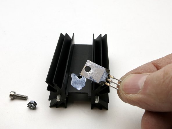
A little heatsink goop is helpful if you have some.
-
1) Attach the Mosfet to the heatsink but leave slightly loose.
-
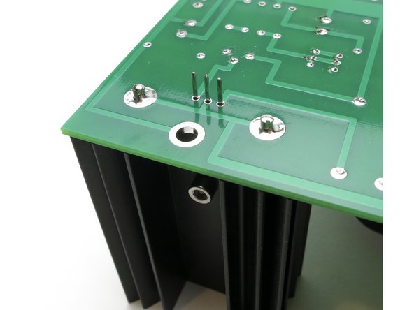
2) Insert Heatsink/Mosfet assembly into PCB.
-
3) Solder heatsink to the PCB first. There's no trick to this, it just takes some time with the soldering iron, as it is a heatsink after all...
-
4) Snug down (modest torque, please don't crank it) the Mosfet attach hardware.
-
5) Finally solder the Mosfet.
-
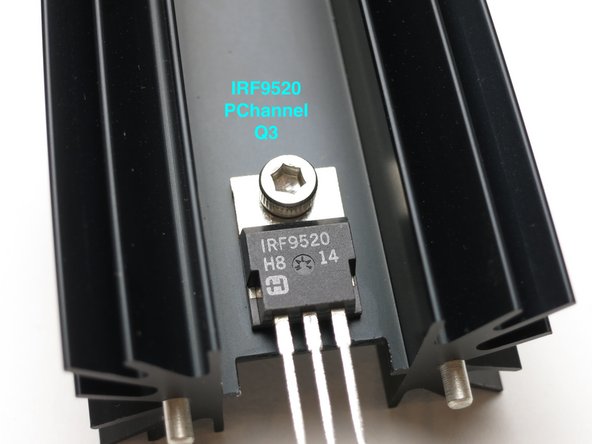
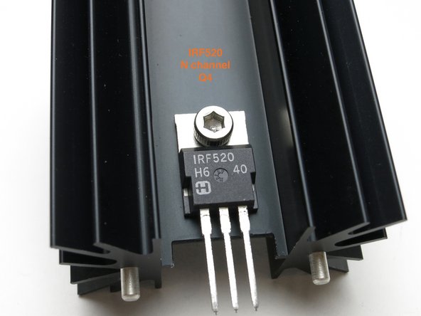
The Q3 positions use the IRF9520 devices. The IRF520 devices are in positions Q4.
-
-
-
Please observe the positions for the power mosfets.
-
IRF520 on the front of the board.(power switch end)
-
IRF9520 towards the back of the PCB. (wiring end)
-
-
-
The provided metal standoffs and their associated screws are used as feet.
-
You may use something else if you choose to, this is DIY after all... :)
-
-
-
Member Charles Port drew this wonderful diagram. Thank you!
-
Refer to article until this guide is completed
-
-
-
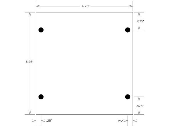
If you want to DIY a base of some sort, here are the PCB dimensions.
-


Cancel: I did not complete this guide.
13 other people completed this guide.