Introduction
What Are We Building?
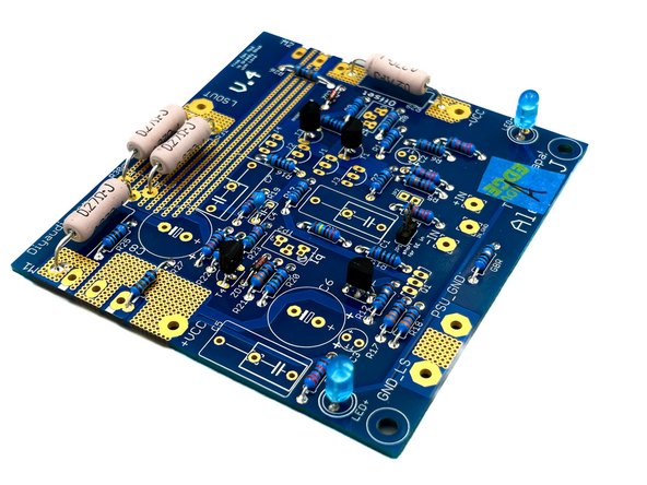
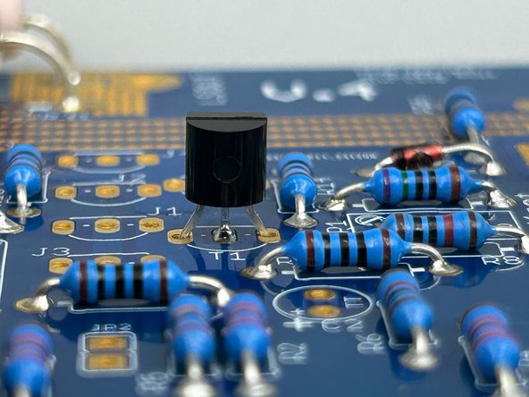
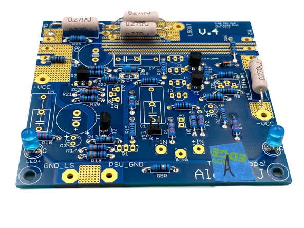
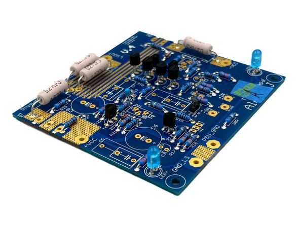
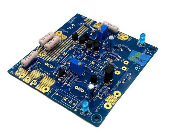
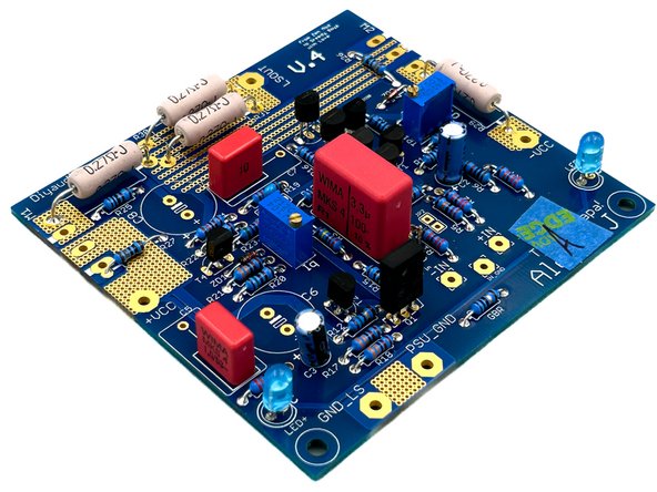
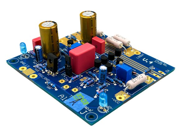
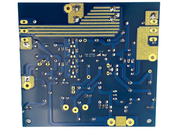
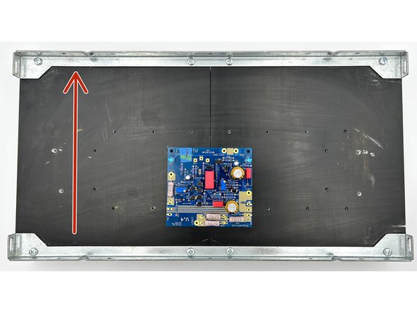
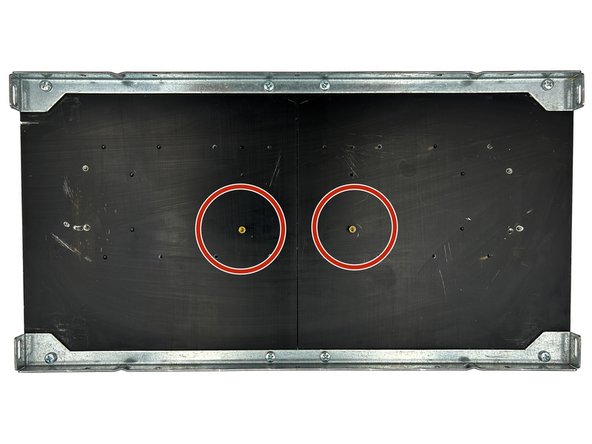
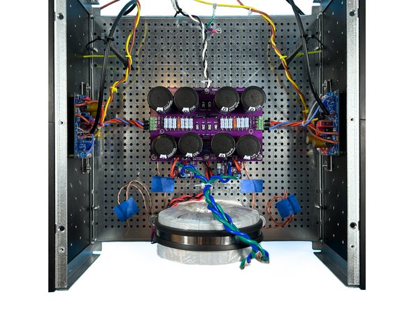
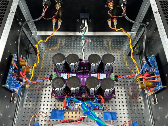
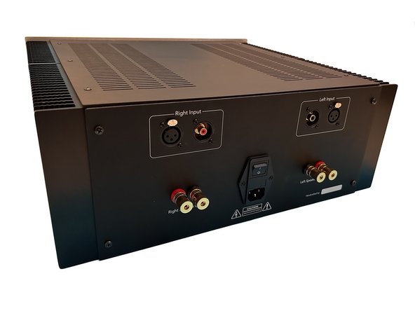
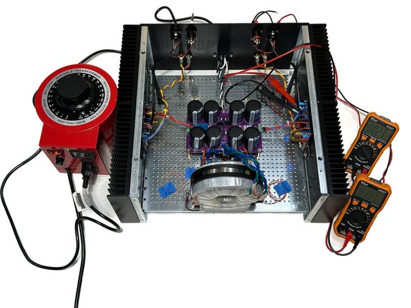
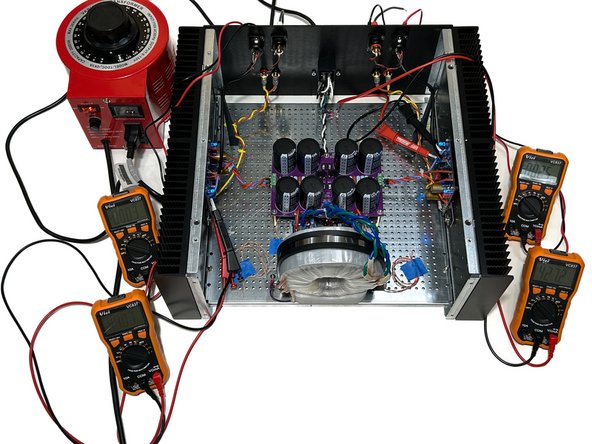
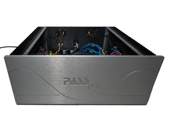
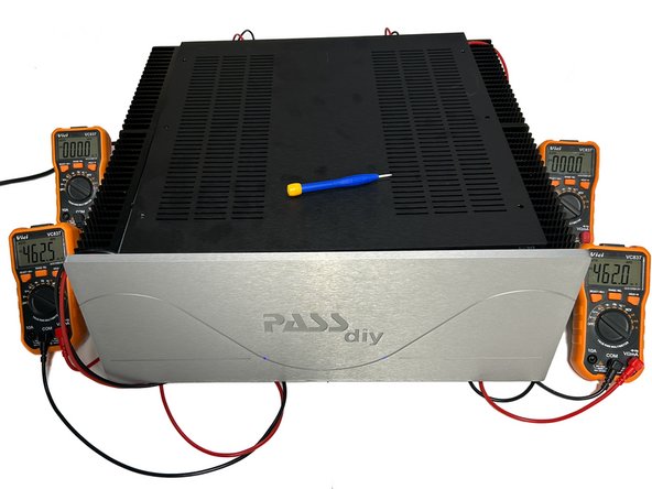
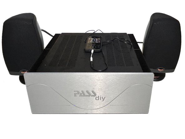
This guide covers the assembly of Zen Mod’s version of the First Watt Aleph J amplifier, aka the AJzm.
|
What Is Covered In The Guide?
This is a build 'guide'. It is not an instruction manual. The purpose is to assist in learning and guide DIYers with helpful information. Builders should not expect every detail to be covered.
|
It is not the only information needed to complete the project. Some additional links are included as guidance. It is critical to understand that the guide is an EXAMPLE of how to complete the project. It is not the ONLY way to complete the project. DIY is all about choosing your own adventure. Have fun!
|
The project is considered moderately difficult. The guide is not intended to instruct someone that has never built an audio amplifier through their first project. This guide is best suited to someone with an interest in audio electronics that has built one or two audio projects, and is ready to take the next step or just needs a few helpful hints.
|
Builders should have a basic knowledge of electronics and should be proficient in through-hole PCB soldering. Although there are many helpful tips throughout the guide, before attempting to build this project, the builder should be confident in their ability to:
- SAFELY work with electronics powered with mains voltage,
- follow a schematic and identify the proper placement of parts from the schematic onto the PCB,
- understand basic measurements to identify parts correctly, and
- properly solder a variety of through-hole components.
|
What Else Do You Need?
There is a list of major parts used in the example, and a list of tools has been provided.
|
Before beginning this guide with the purpose of completing a full amplifier, the builder should have a functioning and tested ~24VDC bipolar power supply capable of 3A continuous output. This guide specifically does NOT cover building your PSU, testing your PSU, or connecting your PSU to mains.
If a power supply has not been chosen, l suggest looking through the forums and asking questions as needed. Popular power supplies for First Watt amplifiers have been made using the Universal Power Supply boards available through the diyAudio store. Universal Power Supply Boards
This build includes the "Stereo Class A Dual Rail Decoupled Power Supply PCB Kit" offered by ThatcherDIYAudio though Etsy.
This guide features parts from the Aleph Jzm parts kit available through the diyAudio store along with the special edition PASSdiy chassis from Modushop.
As necessary, sources for other parts used in the guide are noted. Links are provided in the Tools & Parts section for examples of most of the tools and parts required to complete this project. Options are limitless.
Enjoy!!!
Tools
-
-
A black bullet is an instruction or valuable information.
-
Everything in this guide is important, but here's how you'll know something is REALLY important.
-
A green bullet is the mark to do something.
-
A yellow bullet indicates a fun fact.
-
Warnings will be noted with a warning symbol and bold, red, underlined text. Pay Attention!
-
Tips and tricks and helpful reminders will be noted with an information bullet.
-
Photo / Image captions and information will be noted with the Photo/Image Icon.
-
-
-
Click on the image to enlarge and read the warnings carefully.
-
Construction of this project requires working with potentially deadly mains voltage. In constructing this kit and following this guide, you agree to assume liability for any injury or damage resulting from exposing you or others to these voltages.
-
This guide demonstrates using a proper enclosure. The builder must have or acquire the knowledge to construct an enclosure isolating mains voltage from unintentional contact.
-
-
-
If you do not possess the skills or knowledge necessary to safely complete this project, STOP! Seek assistance.
-
Never assume that shock hazards have been alleviated, even when the unit is not powered. Capacitors can store a lot of energy.
-
Use clip leads for your DMM. Attach and remove the leads with the circuit de-energized. DO NOT connect leads with the unit under power. Disconnect the mains power whenever it is not strictly required for testing.
-
Wear proper PPE including rubber-soled shoes and safety glasses. Work on a concrete or hardwood floor. DO NOT work around water or other liquids.
-
-
-
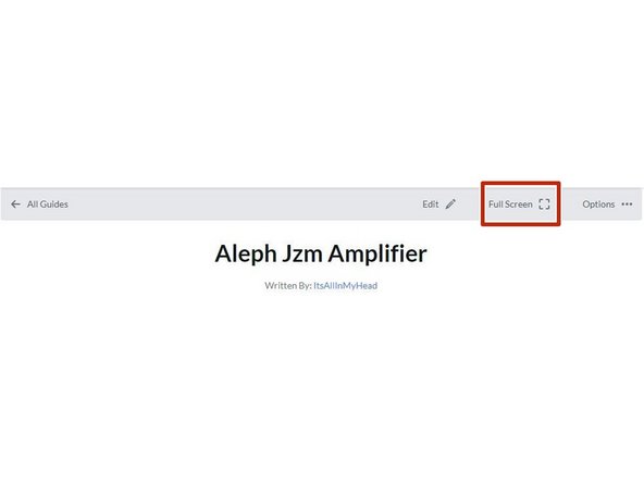
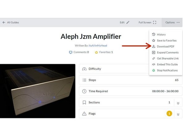
Your first "real" black bullet. You may notice that you have the option to view in "Full Screen". I like it either way, but I prefer full screen. This web platform works well with tablets too. I've tested it with various monitors of various aspect ratios and tablets. Choose what looks best to you. The printed .pdf format is nice too.
-
Image 1 - If you don't know how to get to "Full screen", take note of the box around "Full screen" at the top of the guide above the header / title. That's where you click to move to Full Screen.
-
Image 2 - If you don't know how to print the document. Note that you can download this guide as a .pdf and print it.
-
In all the on-line views, if there are multiple images and/or photos within a step, mouse-over or tap/click as appropriate to make which ever one you'd like the primary image (the biggest one).
-
Mousing over / tapping on the primary image will change the cursor to a magnifying glass. Clicking / double tapping will open a new tab or enlarge and center the image on your screen.
-
In full-screen mode, the keyboard right and left arrows or clicking the arrows in the upper right will advance or reverse one step.
-
Your first "real" green bullet. Choose if you want to view in full screen or standard (if you haven't already) and/or print a copy of the guide.
-
Get started. Move on to step 5.
-
-
-
All mistakes are preventable, and this guide moves slowly through each step.
-
The most common issues with builds are mis-stuffed parts and poor solder joints.
-
Symptoms from mis-stuffed parts typically manifest quickly. For this build, pay particular attention to the small resistors and the TO-92 packaged transistors. The impact from an improper part placement can be benign, or you could release the "magic smoke".
-
The impact of poor soldering varies. A short/bridge that will impact your build is unlikely, but can be catastrophic. More commonly, the issues are partial coverage or a cold joint. Symptoms may not manifest until you least expect them, and they may be intermittent. Inspect each and every joint under magnification. You'll be glad you did.
-
DMM issues can lead to frustration.
-
Check the batteries. When in doubt, replace the batteries.
-
Make sure your probes are reading "0 Ohms" resistance probe to probe or are appropriately compensated.
-
Make sure your probes are connected properly. For this guide, the polarity of the voltage being read isn't critical, but it's best practice. However, as an example, if you are troubleshooting an issue, it is likely that the polarity will matter. Remember this with kindness when you see Photo 1, Step 63.
-
-
-
The most common action you'll take throughout the guide is to "install" your parts AKA stuff the PCB. Parts installation includes:
-
Ensuring you have the correct parts to match the PCB silkscreen / schematic.
-
Ensuring the leads are bent to the proper pitch (if applicable).
-
Inserting the part into the boards along with any vertical spacing (as noted and applicable).
-
Soldering the parts into place.
-
Cutting the leads to the proper length*
-
It is also acceptable to clip the leads to the correct length prior to soldering. There are compelling reasons to do it either way. If you are unsure, watch a few videos, read a few articles, and do some test soldering of your own to see what works best for you. If you choose to clip prior to soldering, use the correct tool.
-
Cleaning and inspecting the joint
-
-
-
This guide does not cover how to solder / install through hole parts. There are a variety of great ways to install a part and achieve a proper solder joint, but there are common themes throughout. Below are a few links. See what works best for you. Neither diyAudio nor the author have any affiliation with any of the companies or persons linked.
-
-
-
-
-
Image 1 - A basic soldering sequence and examples of both good and poor joints. Taken from the Rayming PCB & Assembly Guide linked above.
-
The key variables to soldering are the type of solder chosen, the tip used, and the tip temperature. These all vary widely between users and are inter-related. If you are new to electronics, the best solution is practice. Scrap electronics and inexpensive parts are a wonderful way to learn.
-
Leaving the iron tip on the joint for longer than around 5 seconds is not a substitute for too small an iron tip or too low a temperature. If you need to reflow a joint, or if the solder isn't flowing, flux is your friend.
-
-
-
The builder must ensure all terminations are done properly for safe and trouble-free operation.
-
It is often discussed whether to solder and/or crimp or whether spade-type connections are worthy of a "good" build. In the author's opinion, a properly-crimped connection using high quality terminations and a proper crimper is an excellent choice. Adding a bit of solder can't hurt, but it will never "fix" an improper crimp.
-
The advantage is that many crimped terminations allow flexibility.
-
The disadvantage is that a proper crimp is only achievable when using a proper tool, and many people don't have a proper crimper for each type of termination.
-
The video linked does an excellent job of demonstrating various crimps. You are strongly encouraged to watch it. Excellent Crimping Video Note - Neither the author nor DIYAudio have any affiliation with the video's creator.
-
-
-
Plan your build. Read this guide a few times before you even take the first part out of the bag.
-
Go slowly. You're not getting paid to do 100 boards a day. This should be relaxing and fun. A lot of errors can be traced back to lack of attention and rushing.
-
The ONLY parts within reach should be for the step you are working on at the moment. Many parts look very similar.
-
Move the boards and your body around to give yourself the best angle to solder each part. Get close to your work and use magnification. A well-lit workspace is important. You don't stand a chance if you can't see.
-
Before moving to the next part, triple check your work. Hopefully you won't make any errors, but it is much easier to remove one part than many to fix an error. Using the included documents and following a basic sequence will assist with error-free construction.
-
Take plenty of breaks and stop at any point confusion or frustration sets in. There are a few recommended stopping points throughout the guide, but stop any time you mentally or physically need to recharge.
-
Try to keep distractions to a minimum. Put the mobile phone out of arm's reach.
-
Neatness counts!!! Take pride in your work. You'll be happy you did.
-
-
-
Print the documentation found at the end of this guide or in the Documents Tab if you are viewing in Full-Screen Mode. Yes, you'll need to go back to the Introduction (full-screen mode) or scroll to the end of the guide to find the documents / documents tab.
-
2 Copies of the schematic
-
2 Copies of the board layout
-
2 Copies of the stuffing and inspection checklist
-
The board layout and the schematic may benefit from scaling or resizing to best fit your printer paper. I like mine to be as large as practical and still fit the page.
-
Label one copy of each Channel A.
-
Label one copy of each Channel B.
-
Tidy up your workspace. Keep in mind that you'll be working with a very hot soldering iron, and it can be easy to misplace parts.
-
-
-
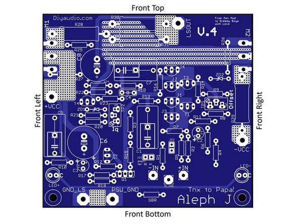
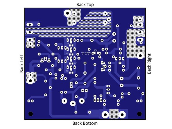
Throughout the guide, the top, bottom, left, right, front, back, or combinations will be referenced. Here is a quick overview.
-
Look over your boards and get familiar with the parts placement. Compare a board to the parts placement document.
-
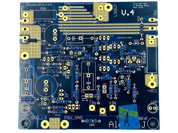
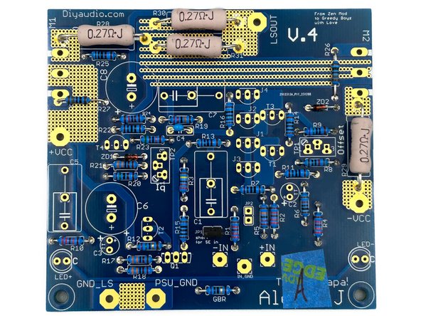
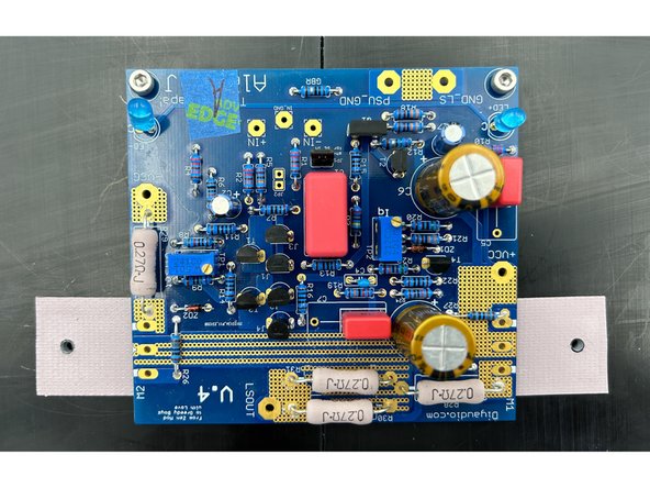
Image 1 - Front view of the PCB. This guide will cover stuffing all the parts with the exception of JP2.
-
The option for JP2 is in place for advanced DIYers that want to bypass C1. Parts were not included in the kit for JP2. Install at your own risk.
-
Image 2 - Back view of the PCB, sometimes referred to as the solder side. You will not install any components on the back of the board.
-
J1' through J4' along with C4' on the back of the boards note SMD pads for substitute components that some advanced builders may choose to try. Those pads are not intended for use with any parts provided in the diyAudio kit.
-
-
-
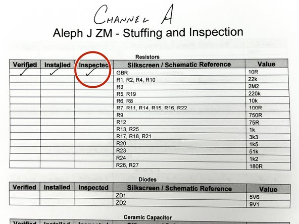
The stuffing and inspection checklist moves in the general flow of installing the shortest parts to the tallest. There are a few exceptions. Experienced builders may choose their own sequence, but we think this works well.
-
Each section of the stuffing and inspection checklist can be done together. It is not important to do each part within a section in order. As an example, I don't install all the small resistors from R1 to R27 in sequence. I install them in groups of the same value. That makes assembly faster and results in fewer errors.
-
For each step, you will be installing all of the parts for both boards. Some people prefer to do one board at a time, but in general, stuffing all of one part for both boards results in fewer errors. In the event of an error, it is likely that both boards will be the same, making troubleshooting a little easier.
-
-
-
It is not necessary to install all the parts in exact order. Within a parts group, my preference is to:
-
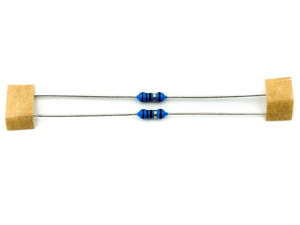
Photo 1 - Remove one set parts from the parts bag. In this case a pair of resistors.
-
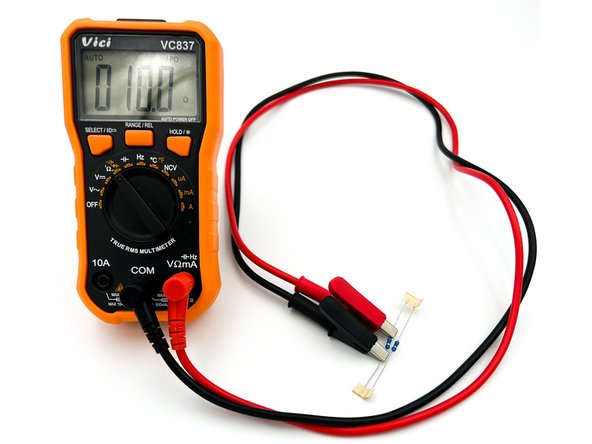
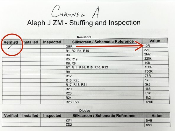
Photo 2 - Measure / validate the part. In this case, measure the resistor with a DMM.
-
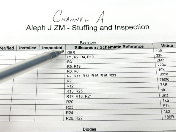
Photo 3 - Validate which part corresponds to the part in-hand using the stuffing and inspection list.
-
-
-
(Continued)
-
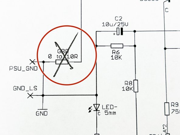
Photo 4 - Validate that the part notation and value match the schematic and cross the part(s) off the schematic.
-
Photo 5 - Note the part(s) value was verified against the schematic.
-
-
-
(Continued)
-
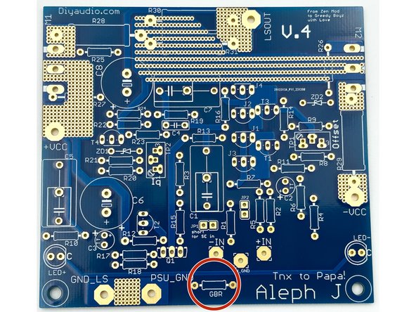
Photo 6 and Photo 7 - Validate the part's placement on the board and cross the part off on the parts placement sheet.
-
This may seem redundant, but it is extremely helpful. Some people find that it is easier to find the location of a part on the parts placement sheet vs. using the silkscreen on the PCBs.
-
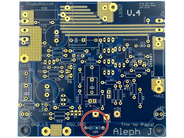
Photo 8 - Install the Part
-
-
-
(Continued)
-
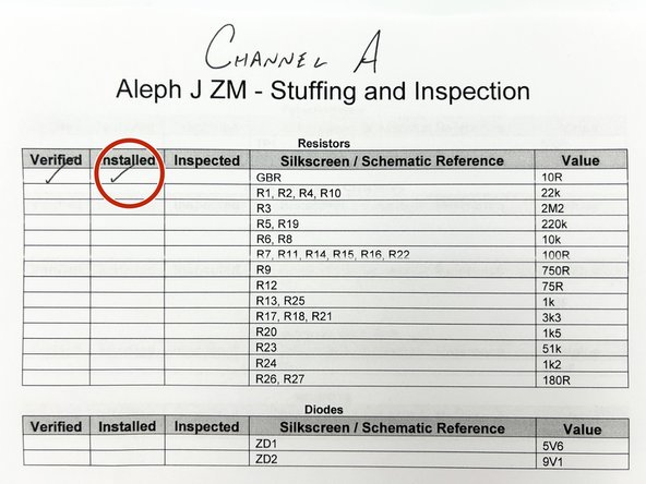
Photo 9 - Note that the part was installed.
-
Photo 10 - Inspect the joints. Clean as needed.
-
Photo 11 - Once everything looks great, note that the part(s) have been inspected.
-
-
-
Most of the kits will have 8 JFETs loose in one of your parts bags. If you received a kit with two bags of 4 JFETs they will be clearly marked, and it will be noted on your packing list. DO NOT MIX the JFETs between the two bags. It's best to keep the JFETs in the bags until you are ready to install them.
-
-
-
Open the bags of parts, verify them against your packing list and get to know what they look like.
-
Place all of your parts carefully in a bowl or somewhere they will not get lost, knocked onto the floor, accidentally spread around your workbench, or mixed in with other parts not associated with this project.
-
Many people like to separate their parts by type. For this project, it's not necessary, but choose whatever method works best for you. It's fairly simple to keep all the parts together and select only what is required for a particular step.
-
-
-
Get to know some of the critical parts in the circuit and how to check them against the schematic and their datasheets. You won't always have a build guide and perfect silhouettes on the PCBs to show you exactly how to place your parts.
-
Image 1 - This is a brief overview of all the transistor types in your kit. Each part type includes an image from the part data sheet and an example of where each type is used in the circuit taken directly from the schematic.
-
Take note - The pinout for the same part type may be different depending on the package. It is always best practice to measure each part and verify the pinout against the datasheet for each part from every different manufacturer.
-
-
-
Review the passive components and the hardware included in the kit.
-
Image 1 - This is a brief overview of all the passive component types and the hardware in your kit. Each part type includes a photo of a representative part of that type and an example of where each type is used in circuit.
-
The nomenclature for resistors is fairly common.
-
The capital R is typically substituted for a decimal place. 0R27 => 0.27 Ohms.
-
k or M may also be noted for kilo or mega. 1k5 => 1,500 Ohms. 2M2 => 2,200,000 Ohms
-
Here is a link to a very helpful tool for 5-band resistor color codes and values.
-
As needed throughout the guide, additional guidance is provided to assist with ensuring proper identification and location of parts.
-
-
-
Review the diodes included in the kit.
-
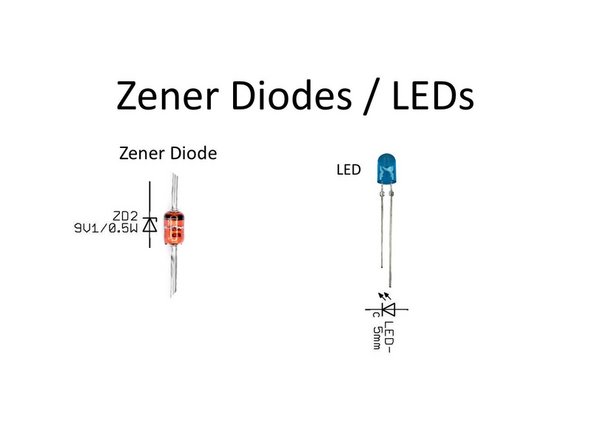
Image 1 - Image 1 - This is a brief overview of the diode types in your kit. Each part type includes a photo of a representative part of that type and an example of where each type is used in the circuit taken directly from the schematic.
-
Note the direction of the Zener vs. the schematic. The board silkscreen has the same marking to assist with proper placement.
-
Note that the short leg of the LED corresponds to the Cathode (c) in the schematic. The cathode is noted with a (c) on the board silkscreen to assist with proper placement.
-
Additional guidance is provided throughout the guide to help ensure proper identification and location of parts.
-
-
-
Tidy up your workspace. Keep in mind that you'll be working with a very hot soldering iron, and it can be easy to misplace parts.
-
Clean both sides of the board with isopropyl alcohol or your favorite PCB cleaner. A dust and oil free board helps the solder to flow nicely. Plus, they're very pretty. Yes, that's real gold.
-
Ambitious DIYers may trace the board with a DMM in continuity mode against the schematic. Don't worry, the boards match the schematics, but give it a try.
-
-
-
Remember to measure the resistance for every part before installation and follow the validation / installation / inspection process.
-
It is helpful to use a lead forming tool. The pitch for all the small resistors except R26 and R27 is 10mm. The pitch for R26 and R27 is 13mm.
-
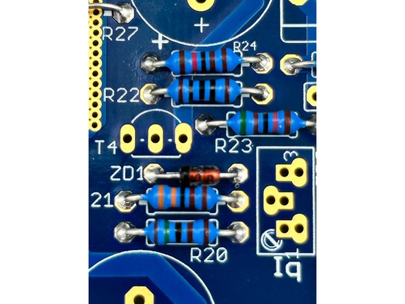
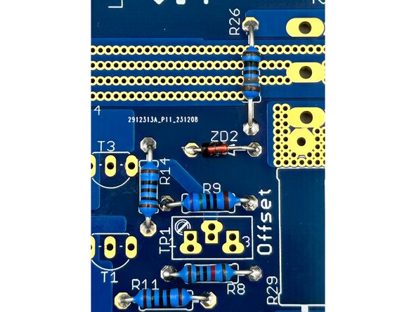
Having all the resistors oriented the same way helps tremendously with troubleshooting. In this build, the bands will read from left to right or bottom to top.
-
Install all the small resistors for both boards.
-
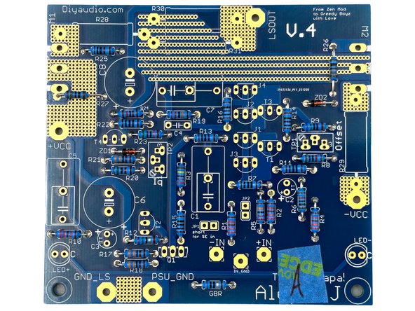
Photo 1 - When all of the small resistors are installed, your board should look like this.
-
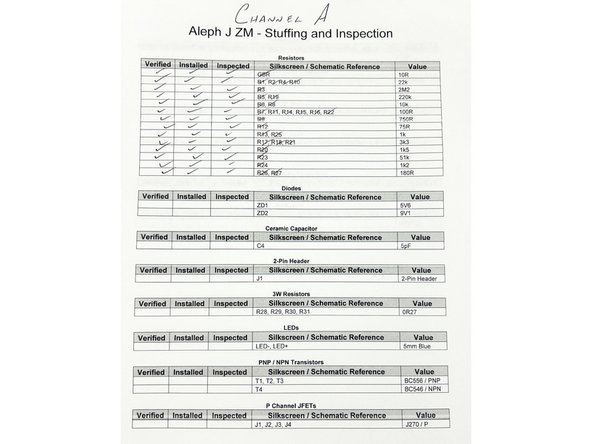
Photo 2 - When all the small resistors are installed, the checklist for one of your channels may look something like this.
-
-
-
Ensure that you properly identify ZD1 and ZD2! Various ways to do this include:
-
Check the tape. For parts included in the kits - one side of the cut tape is red (noting the side of the anode) and one is typically white. For the 5V6 Zener, the white tape is marked with black marker.
-
Inspect them visually under magnification. The print is tiny and not always very clear. ZD1 will have a "23 2B" marking. ZD2 will have a "9V1 BZX 55B" marking.
-
Measure the breakdown voltage. Here is a nice video. https://www.youtube.com/watch?app=deskto...
-
A lead forming tool is helpful. The pitch for both Zener diodes is 8mm.
-
Ensure that you orient the diodes properly per the photo!
-
Install the Zener Diodes for both boards.
-
Photos 1, 2, and 3 - Zeners Installed, ZD1 orientation, and ZD2 orientation.
-
-
-
That was a lot of components. By this point, if you haven't already, take a break.
-
Wise and careful builders will have noted that each and every part or part group has been verified, installed, and inspected on their stuffing and inspection checklists.
-
This is also a perfect time to give the back of the boards a bit of a scrub if you haven't been meticulously cleaning each joint as part of your inspection process.
-
-
-
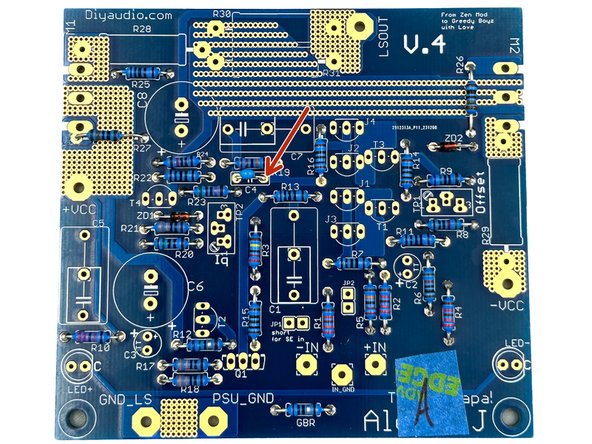
C4 is the small, blue 5pF, ceramic capacitor.
-
Install C4 for both boards.
-
Photos 1 and 2 - C4 Installed
-
-
-
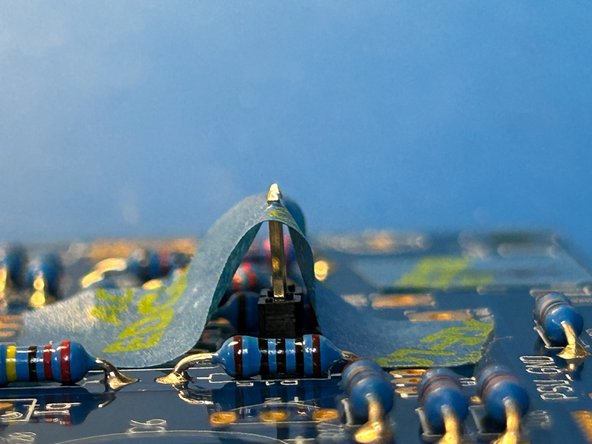
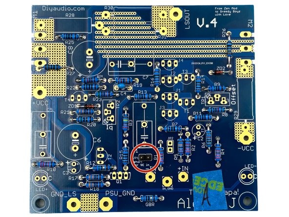
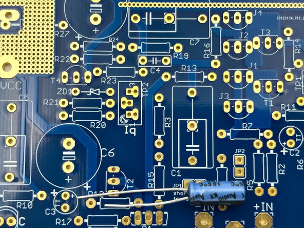
Install the two-pin header for JP1 for both boards.
-
Photo 1 - A piece of tape is handy for holding the part in place while soldering. Tack one lead in place and check that the part is seated firmly before soldering the second lead.
-
Photo 2 - JP1 header installed
-
Put the jumper cap on for safekeeping. Options for using the jumper will be covered later in the guide.
-
Once again, do not install JP2 unless you are certain of the function, purpose, and the risks associated with its use. Consult your friends in the forum if you are uncertain.
-
-
-
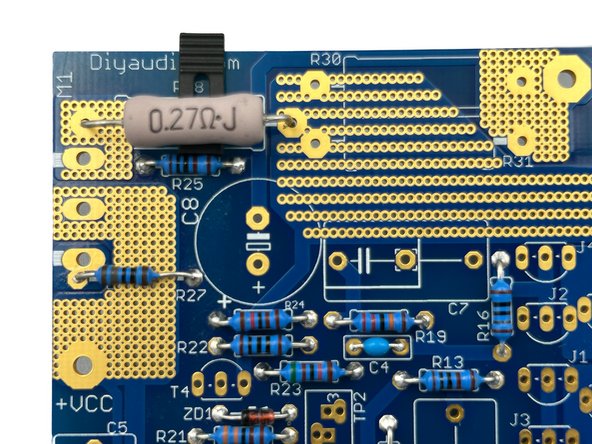
Note - When measuring the resistance of the 0R27 resistors, you're likely not going to get a very accurate reading unless you've got an expensive DMM and know how to use it properly. Handheld DMMs usually struggle below 1 Ohm. Don't worry about it. The value is marked, and they are the only big resistors in the kit.
-
A lead forming tool is helpful. The pitch for all the large resistors is 23mm. Bend the leads, so the value will be facing up when the resistor is installed. It's good practice. Neatness counts!
-
The silkscreen for R31 is mostly obscured. This is a fantastic opportunity to use the parts placement document (which is obviously at hand) to verify placement.
-
Depending on your soldering iron and your choice of tips, this is an opportunity to use that big chisel tip you've been staring at. Go full-send, give 'er the beans, and put the heat to it. There is no harm getting some solder on the adjacent holes / vias.
-
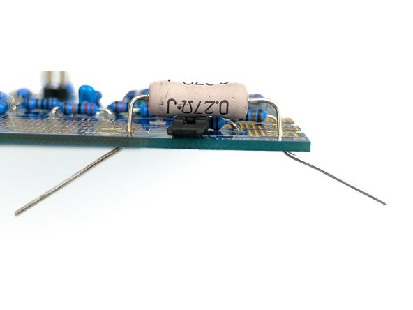
Photos 1 and 2 - These resistors get hot. Raising them above the PCB allows air to flow around them, which keeps them a little cooler. You can use whatever you have around to raise them. In this case the jumper cap for JP1 made a nice spacer.
-
Install the big, 3W, 0R27 resistors for both boards.
-
Photo 3 - Your boards should look a lot like this. A touch more solder was added to R30 and R31 after the photo. Photos are a wonderful tool for inspection. The author should also remember to inspect both sides of the joint EVERY time.
-
-
-
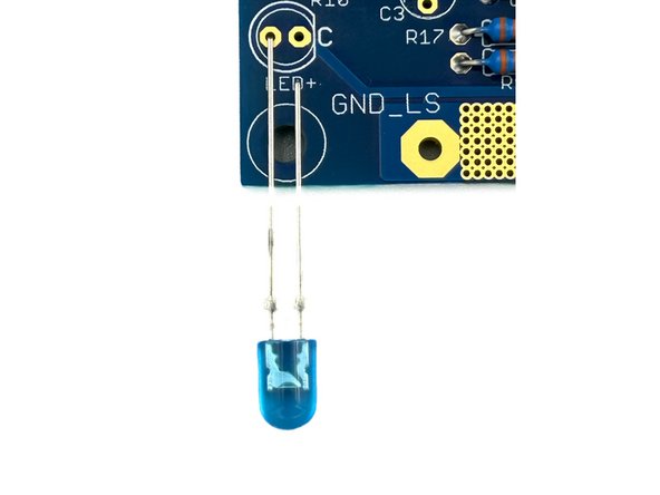
Note - On the PCB, the cathode, the short leg of the LED, is marked with a "C". The LEDs included with the kits are oval and do not have a "flat" side. Said another way, the longer of the two legs is inserted away from the "C".
-
Photo 1 - Note the orientation of the legs relative to the "C".
-
DO NOT use the relative size of the Anvil and Post to determine anode and cathode; you'll likely get it backwards.
-
The LEDs do not sit flush with the boards. Do not try to force fit the parts.
-
Install LED+ and LED- for both boards.
-
Photo 2 - Your boards should now look like this.
-
These LEDs light indicating that the boards have both a V+ (LED+) and V- (LED-) supply connected and powered. The + and - do not indicate the polarity of the LEDs.
-
-
-
Your kit comes with 3 types of parts in a TO-92 package. They all look similar to the naked eye. Even though we've made it very easy for you to differentiate the parts with no measurements. It is critical to good practice to measure / validate each part. Best practice is to check the case marking and measure the part.
-
Note - We have validated that all the silhouettes of the parts on the silkscreens are properly oriented for the parts supplied in the kits. However, you may not always be working with a kit.
-
-
-
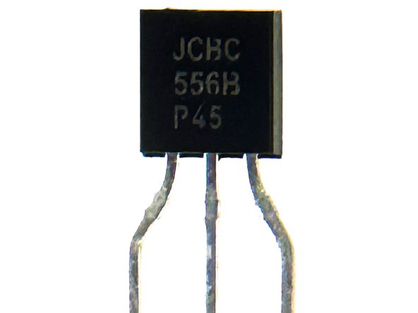
The PNP BJTs for T1, T2, and T3 are on a strip of 6 parts. That may not always be the situation. Here is what the case marking looks like along with how it measures in a typical, basic component tester.
-
Photo 1 - Case marking for the BC556
-
Note - The Date / Lot Code may not match exactly to the photo.
-
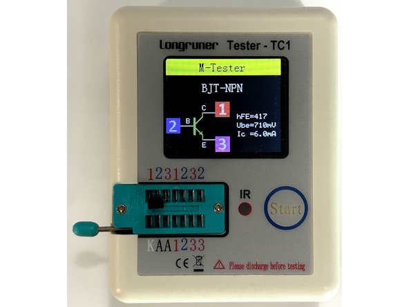
Photo 2 - Basic Component Check
-
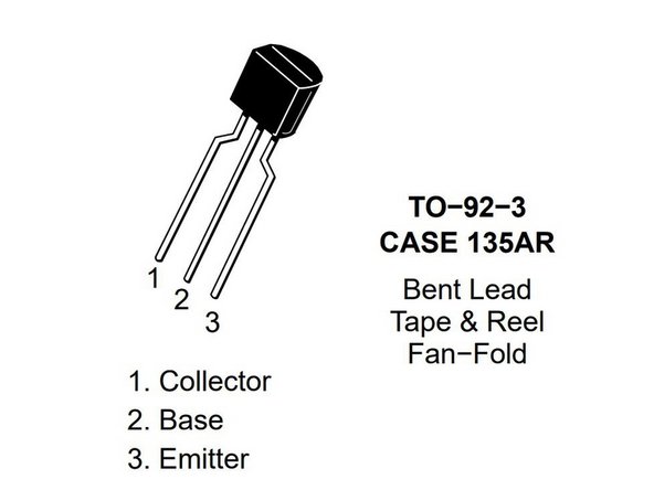
Image 3 - Ambitious and experienced builders always reference the datasheet for all active devices.
-
-
-
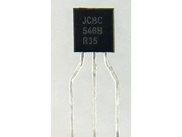
The NPN BJTs for T4 are on a strip of 2 parts. That may not always be the situation. Here is what the case marking looks like along with how it measures in a typical, basic component tester.
-
Photo 1 - Case marking for the BC546
-
Note - The Date / Lot Code may not match exactly to the photo.
-
Photo 2 - Basic Component Check
-
Image 3 - Ambitious and experienced builders always reference the datasheet for all active devices.
-
-
-
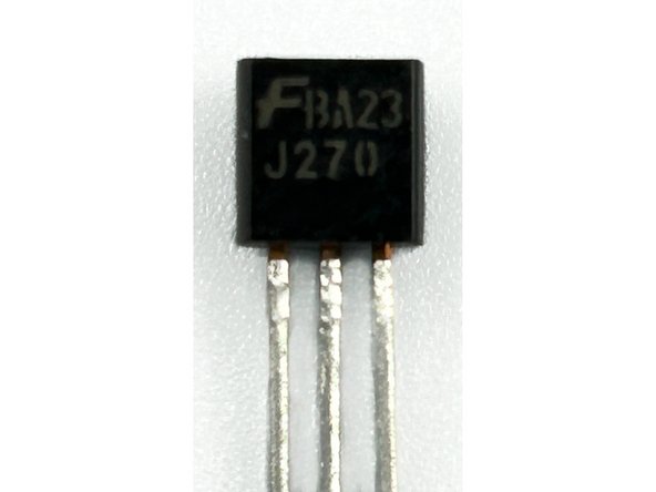
The P-Channel JFETs for the input stage are what put the "J" in Aleph J.
-
If you received two separate bags of JFETs they will be marked. DO NOT mix the parts between the bags.
-
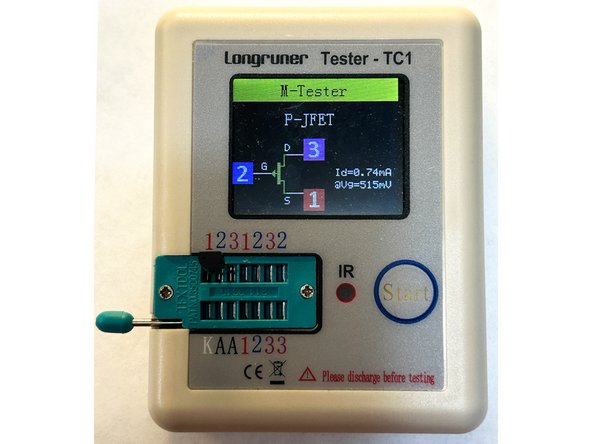
The P Channel JFETs are loose. Here is what the case marking looks like along with how it measures in a typical, basic component tester.
-
Photo 1 - Case marking for the J270
-
Photo 2 - Basic Component Check. As long as it shows as a P-Channel JFET, it's correct. An inexpensive component tester will likely indicate the same pinout even when the part reversed. If you'd like, reverse the JFET and see if you get the same reading.
-
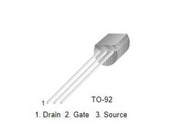
Image 3 - Ambitious and experienced builders always reference the datasheet for all active devices.
-
-
-
DO NOT REMOVE THE NPN AND PNP TRANSISTORS FROM THE STRIP AT THE SAME TIME.
-
Match the orientation of the parts with the silkscreen on the PCB.
-
Photo 1 and Photo 2 - I like to insert the part, bend the legs slightly, and solder the middle leg. If it's not aligned to my satisfaction, I can easily re-heat the joint and adjust. Solder all three legs after it is aligned to your satisfaction.
-
Install T1, T2, and T3 for both boards.
-
Install T4 for both boards.
-
Photo 3 - Your boards should look like this.
-
-
-
Remember - These are your matched sets of JFETs. Take particular care to ensure their proper installation.
-
If you have 4 JFETs in your bag with the rest of the components and another bag with 4 additional JFETs, use one set of 4 for each amplifier board. DO NOT MIX THEM BETWEEN CHANNELS.
-
I like to install them from the 'middle outward'. This area of the board can be a little tight. So, I try to make sure I have easy access to each pad. As an example, I installed them in numerical order - J1, J2, J3 and lastly J4.
-
Some people like to install the JFETs as tall as practical with just a little bit of the lead through the back of the board. This allows them to possibly remove and reuse the rare parts for other builds. It is up to the builder to make their own choice.
-
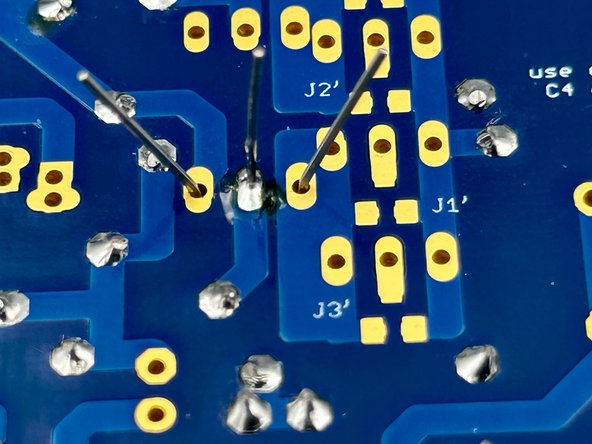
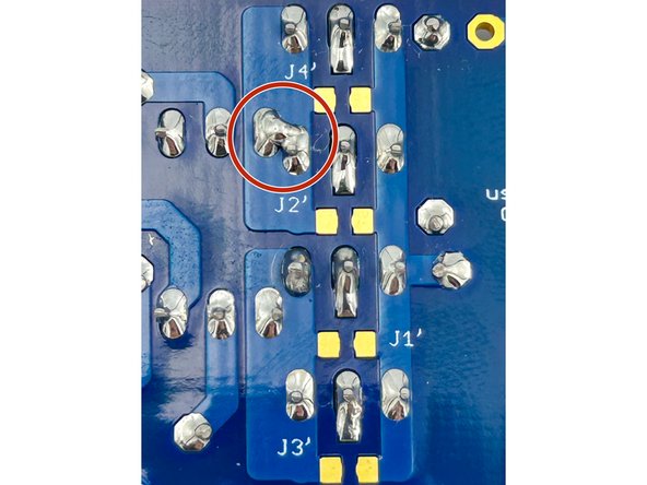
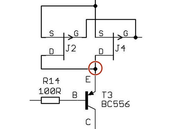
Photo 1 and Image 2 - Don't worry if you bridge the drain of J2 with the emitter of T3. They share the same pad for all intents and purposes... and look at the schematic. I may have overdone it a little for effect. :)
-
Ignore the notations for J1', J2', J3' and J4' along with the extra pads on the back of the board. Those are for those adventurous souls that may want to try out SMD JFETs. That is not in scope for this guide.
-
Install the P-Channel JFETs on both boards - J1, J2, J3, and J4
-
Photo 3 - Your boards should look like this.
-
-
-
It is critical to identify and separate TP1 and TP2. There are a number of ways to do this:
-
Visually
-
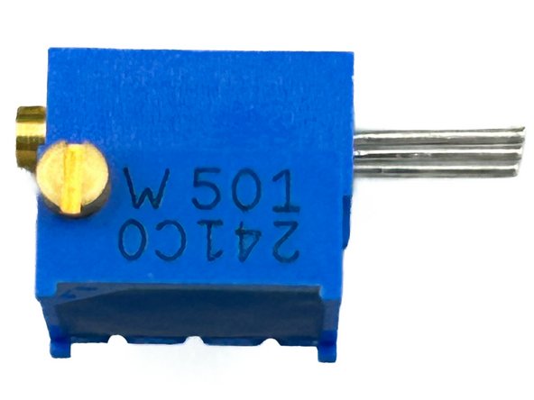
Photo 1 - TP1 is identified with W501. The meaning is 50 followed by 1 zero => 500 Ohms.
-
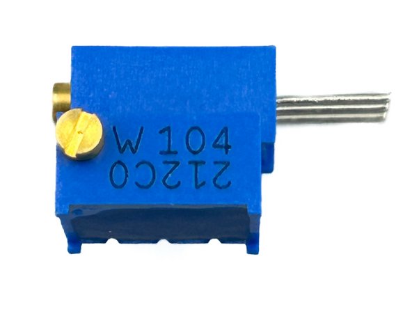
(Photo 2) TP2 is identified with W104. The meaning is 10 followed by 4 zeros => 100,000 Ohms
-
Measurement
-
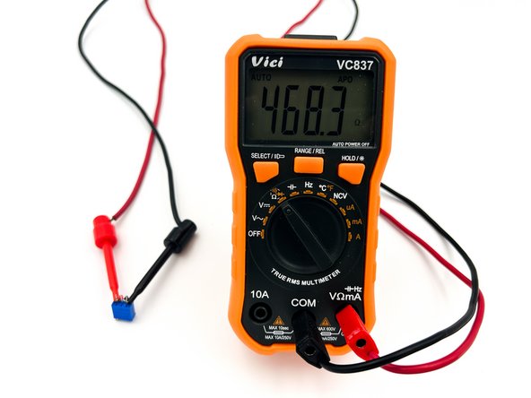
Measure the resistance between the two outer pins of the potentiometers. The value should be within 10%
-
Photo 3 - Example of checking TP1.
-
Separate TP1 and TP2 - It might be helpful to also label the top of TP1 with an 'O' for offset and mark TP2 with an Iq (quiescent current / bias). The silkscreen on the boards might be hard to read. Ensuring you turn the correct pot makes adjustments go more smoothly.
-
-
-
The pots should come roughly centered. However, you should verify that they are roughly centered:
-
Measure the resistance between either outer pin to the middle pin (the wiper) and jot it down.
-
Measure the resistance between the other outer to the middle pin (the wiper) and jot it down.
-
Compare the two readings. If the two readings are roughly equivalent (within 20%), then that is perfect. If not, adjust the pot until the values are within 20%. You'll quickly determine which way to turn the pot. Don't agonize. Close enough is perfect.
-
-
-
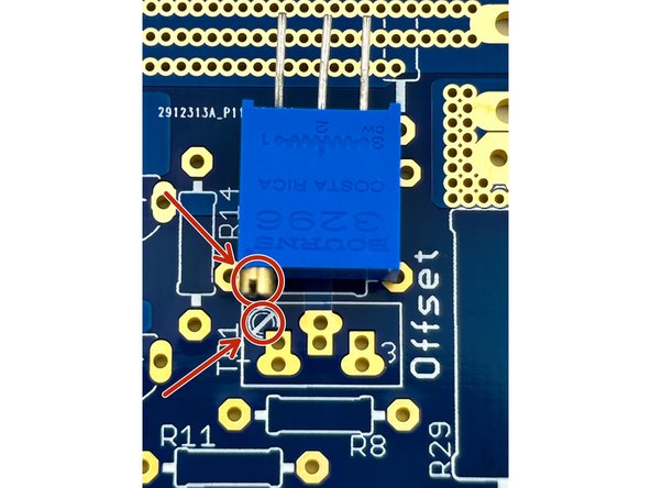
Photo 1 - The PCBs have a clear silhouette noting the proper placement of the potentiometers. The adjustment screw should align with the image on the silkscreen.
-
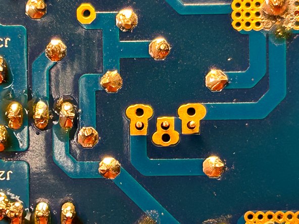
The pads for the pots support many different pin orientations. These pins are in-line and go in the center holes.
-
Photo 2 - Proper holes for potentiometer pins.
-
Similar to almost all parts with 2+ pins, I like to tack one pin into place and ensure that I have the part inserted and oriented properly before soldering the rest of the pins.
-
Install TP1 on both boards
-
Install TP2 on both boards
-
Photo 2 - Here's how it should look.
-
-
-
Verify the orientation of the electrolytic capacitors! The negative side a.k.a. the cathode is indicated with a band. The cathode lead is the shorter of the two leads. The positive side a.k.a. the anode is the longer of the two leads.
-
Photo 1 - Long lead goes into the hole marked with the +.
-
Install C2 and C3 for both boards.
-
Photo 2 - Two caps installed.
-
-
-
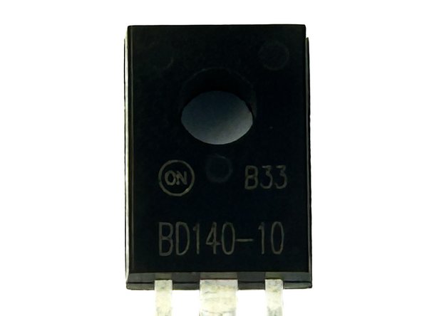
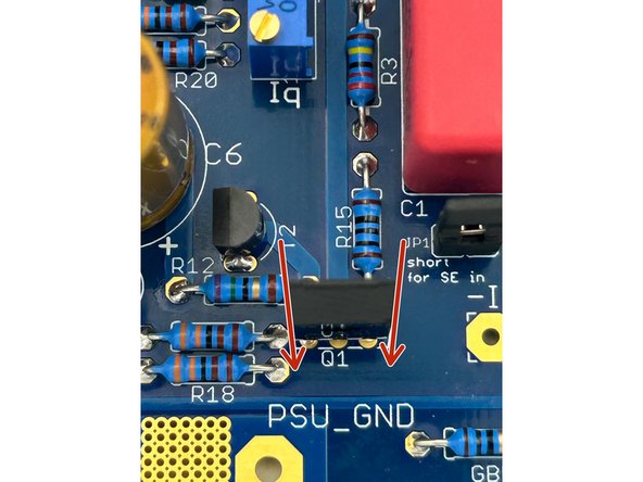
Verify the orientation of Q1! There are a number of ways to do this, but how I do it is to:
-
Match the silhouette on the silkscreen with the profile of the part paying particular attention to the slight taper.
-
Photo 1 - Notice that the part is marked on the face. The face of the part faces the bottom of the board.
-
Install Q1 on both boards.
-
Photo 2 - Note the narrow side of the taper faces the bottom of the board. The lettering also faces the bottom of the board.
-
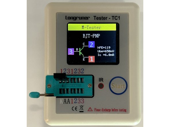
Advanced and savvy DIYers may check the schematic against the data sheet of the part. They may check the part in their transistor tester to ensure that it is a PNP BJT and identify the Collector, Base, and Emitter.
-
Photo 3 - Basic Transistor Test
-
-
-
You get a break. You can install the film caps in any orientation, and it is easy to tell them apart by:
-
Size - The 3.3uF parts are bigger than the 1uF.
-
Markings - The values marked on the parts are legible.
-
Quantity - You should have more of the 1uF in the parts kit.
-
A piece of tape is handy for holding the part in place while soldering. Tack one lead in place and check that it is flush to the board before soldering the second lead.
-
Install C5 and C7 on both boards.
-
Install C1 on both boards.
-
Photo 1 - It's starting to look really nice now!
-
-
-
The process for the big electrolytic capacitors is essentially the same as for the smaller ones.
-
Verify the orientation of the electrolytic capacitors! The longest leg goes into the hole marked with +. The band faces away from the +.
-
Install C6 and C8 on both boards.
-
Photo 1 - Nice, huh!
-
-
-
Give yourself a pat on the back. Nicely done!
-
At this point in your build, every part on your checklist except the MOSFETs should be noted as verified, installed, and inspected. If not, go back and verify each component.
-
You've seen in a few photos that I don't necessarily clean each joint after I solder it. As long as I can inspect the joint properly, I do a section at a time. Now is also a perfect time to get the backs of both boards spotless and inspect all the joints one last time under magnification.
-
Give the boards one last scrub and inspect each joint one more time.
-
Photo 1 - I think these look pretty good.
-
Touch up any joints as necessary and sign off on your own work.
-
-
-
The examples provided show a typical build using:
-
Heatsinks pre-drilled for the Universal Mounting Specification (UMS) pattern,
-
Keratherm electrically insulating thermal pads. Due to heat dissipation per device in this build, if you are unsure of what to use, Keratherm is strongly recommended.
-
Board Mounting and MOSFET mounting hardware included in the "Back Panel Parts Kit"
-
The decisions you make regarding thermal pads / insulation materials and standoff height are essentially fixed after the MOSFETs are installed. Ensure you have all the right parts.
-
-
-
One "side" of a heatsink may be one or two pieces. The example shown is from the Modushop 5U Deluxe chassis and is two pieces per side. It's been through a few projects.
-
If this is the first time you are using your heatsinks, ensure all tapped holes are free from burrs. I use a finger tip to check. In the rare event you find a burr, a small piece of wet-sand paper or a very fine file will remove the burr. Be careful that you don't gouge the sink or damage the threads.
-
Place a PCB on the heatsink in the center. It should be quickly evident that the two mounting holes in the PCB easily line up with the holes on the heatsink (YAY UMS!). This is only a temporary mount to the heatsink to install the MOSFETs. So, don't worry if you don't pick the perfect spot.
-
Photo 1 - This is where my boards mount. Note the orientation of the heatsink vs. the lettering on the board. Ideally, the MOSFETs should be on the lower portion of the heatsink. The arrow points to the top of the heatsink. At this point the left and right channel or front and back do not matter.
-
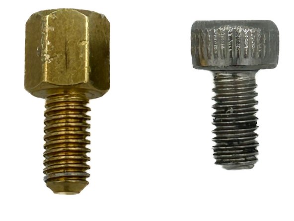
Install two standoffs into each heatsink to line up with your mounting holes on the PCBs.
-
DO NOT over-tighten the standoffs. Overtightening will result in breaking the threads off, and you will be VERY sad. Firmly finger-tight is perfect. If the threads stick, back it in and out. A little lubricant may help also.
-
Photo 2 - Here is where my standoffs are mounted.
-
-
-
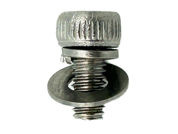
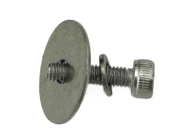
Mount the PCBs with the short screw, a split washer, and a flat washer. Don't tighten it yet. Just a few threads to hold it in place is fine.
-
Photo 1 - Short screw and standoff. The angle of the photo isn't super. They were sitting right next to each other, but the screw looks much bigger than it should relative to the stand off. It's also how I take my fishing pictures.
-
Photo 2 - Screw, split washer, and flat washer. That is the proper order.
-
Note - The back panel kits from the diyAudio store do not include split washers. Any M3 split washer will work perfectly.
-
-
-
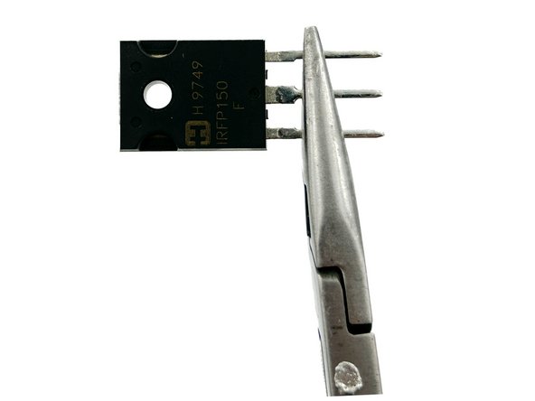
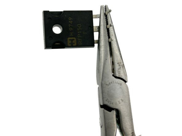
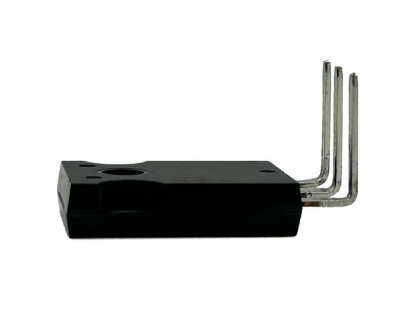
Photos 1, 2, and 3 - It's simple to get a proper bend in the MOSFET legs. Grasp the part just below the narrowing point and bend until the legs are at 90 degrees.
-
Ensure that the lettering is up and the metal tab is down. It's easy to adjust them a little, but bending them back in the entire opposite direction can be a problem.
-
Bend all three leads of your MOSFETs to a 90 degree angle as shown. They don't need to be perfectly 90 degrees. Just get it close.
-
-
-
There are a number of ways to get the MOSFETs and the Keratherm into place. Use your preferred method or follow along.
-
Photo 1 - I place the Keratherm on the heatsinks aligning the holes first as shown.
-
Then I lift the board gently and slide the MOSFET legs into the holes.
-
Photo 2 - Then, I gently move the Keratherm back into place if it has shifted.
-
-
-
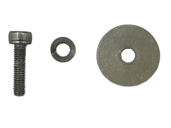
Photo 1 - Hardware for mounting the MOSFETs to the heatsinks.
-
Photo 2 - The split washer always goes next to the screw head, then the fender washer.
-
Note - the back panel parts kits from the diyAudio store do not come with split washers. Any M3 split washer will work perfectly.
-
DO NOT tear or puncture the Keratherm with your screw or stick anything sharp in the hole to try and move the Keratherm. The hole will naturally enlarge a little, but the Keratherm must be fully intact. If you need to move it, take your time and move it gently from the edges. DO NOT try to wiggle it into place with the screw.
-
Photo 3 - I gently insert the screw into the hole to make sure I did not catch the Keratherm. I thread it with my fingers first to ensure I don't cross-thread the holes or have any of the Keratherm caught on the screw. Then once I know everything is aligned properly, I tighten the screw with an allen key to just over finger tight.
-
Fancy people may use a torque wrench set to 1.1 Nm per the datasheet, which I'm sure you've all read.
-
Dry fit all of your MOSFETs and tighten them to the heatsinks. DO NOT solder them yet.
-
Tighten the boards to the standoffs using an Allen key until just over finger tight.
-
-
-
The keen-eyed observer will note that this is not the same heatsink from the previous steps. No worries. This step was inserted for added clarification. It's a heatsink for a 4U/400 chassis.
-
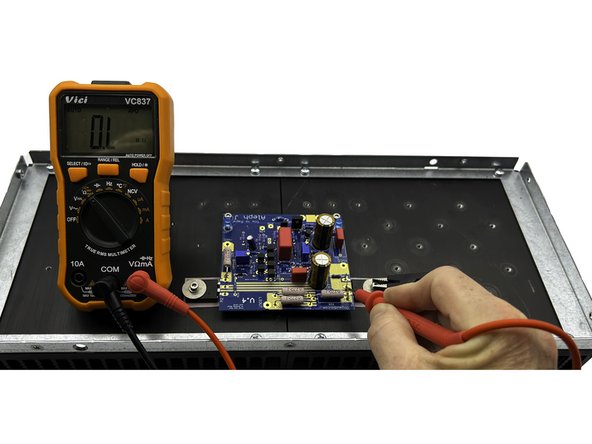
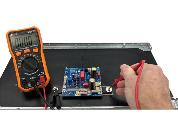
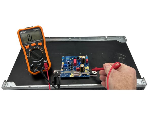
It is wise to check the resistance from the heatsink (chassis / mains earth) to each pin of the MOSFETs prior to soldering them into place. The metal back of the MOSFET is the drain, and it must be electrically isolated from the heatsink. Take the extra few seconds and check all three legs.
-
With the DMM set to resistance, (if you do not have an auto-ranging meter, set it to the highest range) check the resistance from each of the legs of both MOSFET to the head of the screw mounting the MOSFET. If the reading is not O.L (over limit) or in the MOhm range, seek assistance.
-
Photo 1 - Meter set to resistance. Probes placed on mounting screw (mains earth / chassis GND) and pin 2 (drain). O.L (A very high resistance) is a proper result.
-
-
-
Give the board a little wiggle and allow it to move up and down the MOSFET legs. Let it settle into place, and give it one last check. It should be level even when resting only on two standoffs.
-
A little preparation can save a lot of heartache! You will be soldering the MOSFETs from the top.
-
With a cold soldering iron, determine how you will get in and out for each leg of the MOSFETs without touching any of the adjacent components. Pay particular attention to R27 and R26. Move the heatsink and your body to give yourself the best chance.
-
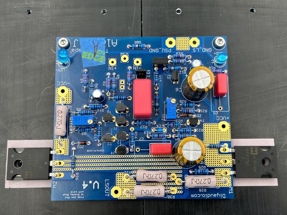
Solder all three legs of all the MOSFETs into place.
-
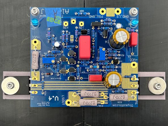
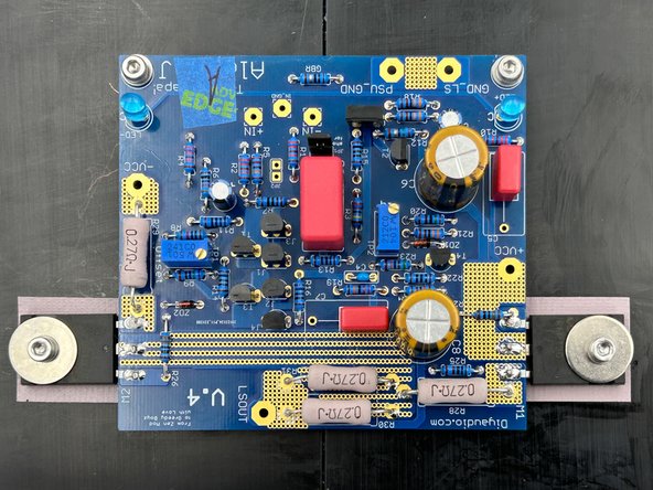
Photo 1 - Your boards should now look a lot like this.
-
Some people trim their MOSFET legs and some don't. I trimmed mine after I soldered each joint to make it easier to solder adjacent legs and give myself more room to work. I soldered the legs from bottom to top in photo 1. If you do trim the legs, pay attention to R27!
-
-
-
The metal back of the MOSFETs, electrically speaking, is the drain. So, it is critical that the metal back of the MOSFETs is not in contact with the heatsinks. The heatsinks are "chassis ground". However, we need the MOSFETs to dump their heat to the heatsinks. Thus, we use Keratherm between the devices and the heatsinks.
-
Keratherm has excellent thermal conductivity (allows the heat to pass from the device to the heatsink), while also being an excellent electrical insulator.
-
With your DMM set to resistance, place one probe of the DMM onto the head of the screw mounting the MOSFET. Keep that probe stationary as you touch each leg of both MOSFETs. Any typical handheld meter should read over limit / open loop. Do this for both boards / heatsinks.
-
Photo 1 - Notice 0 Ohms resistance between the two screws mounting the MOSFETs. They are at equal potential at "chassis ground". If your meter reads a few ohms or more, it's fine. Depending on your meter, it may not be a static reading (it may bounce around).
-
Photo 2 - Demonstration of the DMM showing O.L. between the chassis ground (the screw mounting the MOSFET) to one leg of a MOSFET. Repeat for the other 5 legs.
-
-
-
You've now completed your amplifier boards and done an initial check to ensure that they mount without issue. It's a perfect time to congratulate yourself and take a break.
-
-
-
The example build uses a specific PSU, and a Modushop 4U/400 chassis. There are a number of chassis options, PSU options, and layout options. I chose to use a few parts created by fellow DIYers. You will likely choose a few different options.
-
It is not necessary (and it's possibly not advisable) to copy this build exactly. Photos are provided for inspiration and ideas only. Make your build your own,
-
Steps 55 to 61 show a few examples. You may choose an entirely different layout based on your chassis size, power supply, personal preferences, or other criteria.
-
-
-
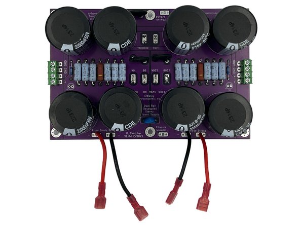
Photo 1 - This is the main PSU board I used, created by fellow DIYer rhthatcher.
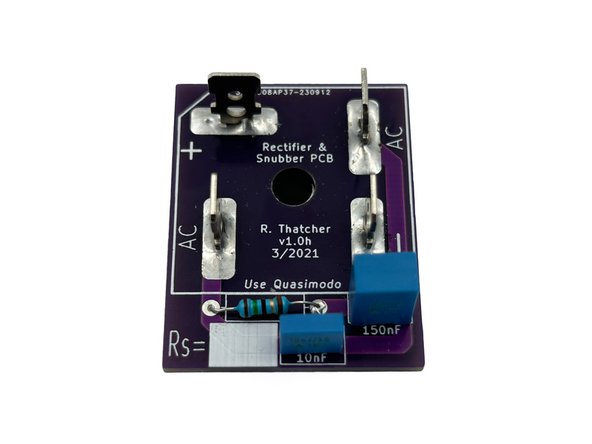
-
Photo 2 - This is one of the rectifier / snubber combination boards I used. It's also created by rhthatcher and included with the main boards.
-
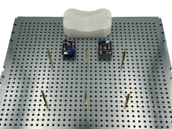
Photo 3 - This photo shows a cool throne to vertically mount a toroid (designed by fellow DIYer, Birdbox) along with a rough layout of where I anticipated the rectifiers and main PSU board being mounted to the perforated baseplate.
-
I moved components a few times and brought in the amp boards mounted on the heatsinks to visualize the DC connections to the PSU and the input and speaker connections to the back panel.
-
Nothing is permanent. Begin to layout your chassis keeping in mind wire routing that may include, but is not limited to:
-
AC Power Wiring - Mains Live, Neutral, and Earth; Transformer Primaries; and Transformer Secondaries.
-
AC Signal Wiring - Input and Speaker
-
DC Power Wiring - V+, V-, and GND
-
-
-
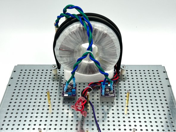
Photo 1 - The transformer is mounted, and the secondaries are connected to the rectifier / snubber boards. Note AC wiring is tightly twisted.
-
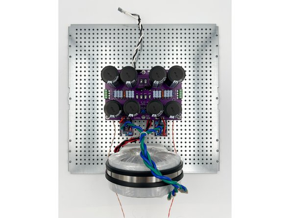
Photo 2 - The overall layout of the completed and tested PSU.
-
The CAT5 twisted pair wiring is for optional front panel power-indicating LEDs.
-
At this point you should have a completed and tested PSU with a target loaded output of around +- 24VDC. Typically ~25-27VDC unloaded.
-
Make sure your PSU is tested and operational. If you need help building and testing a PSU, you can find a tremendous amount of guidance from your fellow DIYers in the forum.
-
-
-
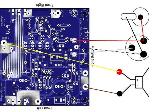
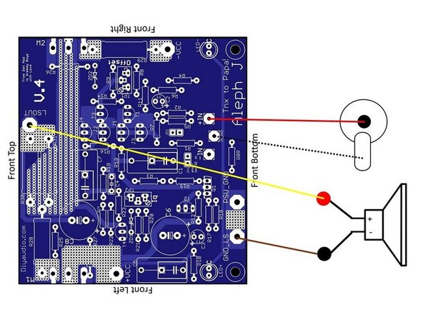
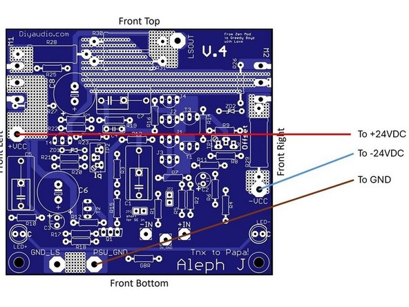
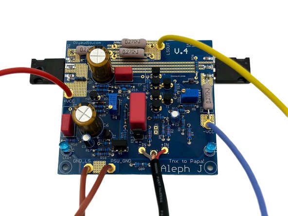
There are a number of ways to connect your amplifier boards to the DC supply, and there are a number of grounding schemes. In addition, there are a number of ways to connect your XLR and RCA jacks. Choose the method that works well for you. If you're unsure, seek help in the forums or follow the diagrams and examples provided here.
-
Image 1 - Basic diagram for the input and speaker wiring (signal wiring) for using both XLR / Balanced and RCA / SE inputs.
-
Image 2 - Basic diagram for the input and output wiring for SE / RCA inputs only.
-
Image 3 - Basic diagram for the DC supply wiring.
-
Remember that if you will be using both RCA and XLR inputs, you will remove the header cap for JP1. When using RCA inputs, you will need to use a shorting pin / plug between pins 1 and 3 of the XLR input. You can buy them from various places or fashion one of your own from some solid core wire. Example
-
-
-
Some people like to wire their PCBs before mounting (Starting at step 44) and installing the MOSFETs. That allows mounting the boards only once. That is perfectly valid. PO-TAE-TOE, PO-TAH-TOE. If you are unsure, ask for guidance. Since you've read the guide a few times before building, you've already made your choice before you got here. :)
-
Now is not the time to be stingy with wire. Unless you are a perfectionist professional and can measure and cut each time perfectly, it's best to err on the side of caution and cut your wiring a few inches or more longer than will likely be necessary.
-
Note - I chose to do both XLR and RCA inputs for this build. Thus, I wired the input for +, -, and GND. If you are ONLY planning to use SE / RCA inputs, you will only wire the + and GND using a two-conductor cable.
-
Color coding is not standardized. I chose Blue for -VCC, Red for +VCC, Brown for both GNDs, and Yellow for LSOUT. The only colors to consider avoiding are black, white, and green. Those are almost always associated with mains power (live, neutral, and earth). Otherwise, choose what you can remember, see clearly, and that makes sense to you.
-
There are a plethora of methods for attaching wire to PCBs effectively. The example shown uses flexible, generic, silicon jacketed 16AWG wire directly soldered to the PCBs for all DC power and speaker connections. Input wiring is Mogami W2552.
-
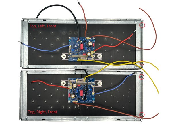
If necessary, remove your amplifier boards from the heatsinks and install appropriate lengths of wire for +VCC, (DC positive) -VCC (DC Negative), GND_LS (Speaker Ground), PSU_GND (PSU Ground), LSOUT (Speaker Out), and input wiring.
-
Photo 1 - Example of board wiring.
-
-
-
The new Modushop chassis come with brackets that fully surround the heatsink. Be careful to note that they have a front and back. The back of the bracket / heatsink that attaches to the back panel is the end with the threaded holes. Make sure you mount your boards appropriately if you have one of these chassis.
-
Choose your appropriate mounting location for each heatsink and mount your PCBs / MOSFETs to the heatsinks. Again, the screws for the standoffs should not be over-tightened, and the perfect torque for MOSFET mounting is 1.1Nm (a bit over "snug").
-
Photo 1 - Wired boards attached and oriented properly on the heatsinks. Note the back side of the heatsinks have the threaded holes (circled in red).
-
-
-
Mount the heatsinks to the perforated baseplate.
-
Tidy up all the wiring. Get it as close to final as practical. Snagging a wire and pulling it too hard unintentionally would be sad at this point in the build.
-
Photo 1 - Example of wiring being roughed in.
-
There are a number of ways to run the speaker and PSU grounds. The method shown is as-designed by ZM himself. Feel free to try any method you know works well for you.
-
V+, V-, and PSU GND are twisted from the amp board to the PSU.
-
LSOUT and LSGND are twisted.
-
Another addition from fellow DIYer, Birdbox; super cool wire management towers.
-
-
-
Reminder - You have already properly tested your PSU, right!?
-
There are a number of ways to terminate and attach speaker connections. Choose your own adventure. I used female spades (soldered to the speaker wire) matching the binding posts included with the back panel parts kit.
-
Mains connections are specifically not covered in this build guide. If you are unsure, seek expert guidance. Improper handling of mains voltages can result in injury or death!
-
Finalize wire lengths. Attach the back panel. Trim, terminate as appropriate, and connect / solder as appropriate all mains wiring, speaker wiring, and input wiring.
-
My preferred method when using Neutrik D-type jacks that come in the back-panel parts kit and for the XLR input jacks I used is to install them from the inside. This allows me to solder the jack to the input wiring prior to installing the jacks on the back panel. For me, that's easier. Plus, it looks spiffy. Feel free to do what works for you.
-
Photo 1 - All wiring complete with the exception of the LEDs for the front panel. Note - both amp boards are connected to the PSU for finalizing wire length and attachment points.
-
Photo 2 - Complete back panel. Nice!
-
-
-
The goal of the next set of steps is to ensure that the circuit is generally functioning properly before buttoning up the chassis and finalizing the settings.
-
It is wise to use a variable transformer for your initial power-up and checks. This guide illustrates using a typical model.
-
If you do not have a variable transformer and cannot get one, it is strongly recommended to do a basic dim bulb check. If you are unsure how to build and/or use a dim-bulb-tester (DBT) properly, ask in the forums.
-
The Aleph J may not behave like you expect when powering up with a variable transformer. Fellow DIYer KevinHeem was kind enough to post a video I made of a typical sequence. Aleph J Bias As Mains Voltage Is Increased Note that the bias rises to a point and then decreases. This is totally normal.
-
It's not strictly necessary, but it is very nice to have at least 2 DMMs. The guide will assume you have at least 2 DMMs. If you don't have 2 DMMs, it is assumed you are clever, patient, and skillful enough to use one.
-
It is almost essential that you have a set of "J-Hook" type probes or small alligator clips for your DMMs. It is much safer to connect the probes and leave them in place for measurements.
-
Triple check your wiring!
-
-
-
Ensure there is no power to the amplifier. If you had both amplifier boards connected to your PSU to finalize wiring, disconnect one channel. Check one channel at a time.
-
Short the inputs. Since I am using XLR and RCA inputs, I left JP1 in place and shorted the RCA jack with a typical 'shorting plug'.
-
With a DMM set to DCV place the (j-hook or alligator clip) probes across R29. Put the DMM common (black) probe on the leg closest to the -VCC supply. If your DMM is not auto ranging, set your DMM so it will register properly for an expected voltage range of 0 to 600mV or so.
-
Connect another DMM set to DCV to the speaker outputs / binding posts. If your DMM is not auto ranging, set your DMM so it will register properly for an expected voltage range of 0 to 600mV or so.
-
With the power off, connect the variable transformer to the amplifier.
-
Ensure the variable transformer is set to the lowest output voltage. It is assumed that you have checked your variable transformer for the range of output voltages and know when you've reached the equivalent to your mains voltage.
-
There will be a number of times where it will be noted to STOP! if you observe something out of the ordinary. STOP! means to carefully but deliberately cut power to the amplifier. Then, troubleshoot and/or ask for help.
-
-
-
Turn on the amplifier power switch, and turn on the variable transformer. You should see close to 0V or <100mV on both DMMs. If you see anything above 100mV. STOP!
-
Gradually increase the output voltage from the variable transformer in stages. If you see a voltage above 700mV across R29, STOP! The full segment below takes <20s for me. Read it a few times again before proceeding. Move deliberately while keeping an eye on the DMMs, but there's no need to creep along.
-
Increase the output to roughly 1/3 of your mains voltage. Pause for a few seconds. Fairly early, you should see your LEDs begin to glow. Both LED+ and LED- should light at a very similar point. If not, STOP!
-
Increase the output to roughly 2/3 of your mains voltage. Pause for a few seconds.
-
Increase the output to full mains voltage.
-
Give the pot labeled Iq a turn CCW and a turn CW and ensure that the voltage across R29 changes accordingly. If your bias voltage is >500mV, turn the pot CCW and reduce the voltage to <450mV. Turn the pot labeled Offset a turn CCW and a turn CW. Ensure the voltage across the binding posts changes accordingly.
-
Turn off the mains power. Disconnect the amplifier board from the PSU. Connect the other amplifier board, and repeat. Once you've successfully checked each board independently shut off the power to the amplifier.
-
Photo 1 - Variable transformer set to full mains output. Front DMM displaying voltage across R29. Rear DMM displaying voltage across binding posts. Note - your results will vary.
-
-
-
Connect the other amplifier PCB to your PSU. Triple check the wiring. Yes, again. It's way too easy to hook up the DC supplies in reverse.
-
Ensure the variable transformer is turned off and set to the lowest output voltage.
-
If you only have two DMMs, connect them to R29 on both channels. If you had no issues with offset in the earlier steps, it is less of a concern. If you have four DMMs, connect them exactly as before.
-
Gradually increase the voltage output to full mains voltage while monitoring the DMMs. Again, if you see anything over 700mV, STOP!
-
Once you reach full mains voltage, allow the amp to settle for a 10 minutes or so. You should see the voltage across R29 drop slightly as the heatsinks warm.
-
Check both sets of Iq and Offset pots, yes again, to ensure they adjust the voltage across R29 and the binding posts properly.
-
Turn off the power. Treat yourself to your favorite snack and beverage.
-
Photo 1 - Full mains voltage. Both channels connected. DMMs across appropriate test points. All voltages under control. Pots tested.
-
-
-
Setting the final bias and nulling the offset should be done at thermal equilibrium in an area that will closely resemble the temperature of where it will live permanently. So, it's time to button up the chassis.
-
Install the front panel and the LEDs (as applicable).
-
Install the feet on the bottom plate (as applicable). Ensure you have the perforated baseplate tightened to the heatsinks. Make sure any wire management that involves getting to the underside of the perforated base plate is complete. Install the bottom plate.
-
User's choice - Power up the unit with the variable transformer one last time to ensure everything looks good... OR... relish in DIY bravado, remove the variable transformer, and power it up.
-
Enjoy the view.
-
Photo 1 - The view is pretty nice, eh!?
-
-
-
The goal of this step is to set the final bias and offset. Final bias setting should be 460mV +- 10mV. The offset should be nulled to 0mV +- 5mV. This needs to take place at thermal equilibrium. It typically takes me at least 2 hours using 2 DMMs per channel. YMMV.
-
The bias of the amplifier decreases as the output devices warm up and begins to drop as soon as the lid is removed. So, overshooting a little is not a bad thing. Offset is very stable, relatively speaking and rarely wanders more than a few mV or even 10ths of a mV once the heatsinks are warm.
-
Install DMMs again on R29 and the binding posts per previous steps. Ensure that inputs are shorted. Rest the top plate / lid gently on top of the amplifier taking care not to yank on your probe leads.
-
Connect mains power directly and power up the amplifier. If the voltage across R29 is between 400 and 500mV leave it alone. If it is not, adjust the pot labeled Iq accordingly.
-
Adjust the pots labeled offset to set the voltage across the speaker terminasl to +- 10mV for each channel. Then let it sit for about 45 minutes.
-
Remove the lid and carefully, but quickly adjust each pot accordingly in an attempt to get close to 460mV across R29 and <5mV across the binding posts. Put the lid back on. Wait at least another 5 to 10 minutes. Remove the lid. Tweak. Replace the lid. Wash, Rinse, Repeat until you're happy.
-
Photo 1 - I'm happy. Close enough to 460mV on both channels and less than a tenth of a mV of offset. I got lucky with 0.0mV on both channels at the time of the photo. It wanders a teeny tiny bit. It took a couple hours, but I was typing this guide too.
-
-
-
It is bad luck to screw the lid down before testing the amplifier with music.
-
Grab a pair of speakers that don't matter much to you or a single speaker to move back and forth. Connect the amplifier to the speakers and a source.
-
I used my phone as a source for initial testing. I left JP1 in place and used the RCA inputs. Then, I removed JP1 and used a balanced source for a check. It's wise to check both sets of inputs if you are using both.
-
Play some music. Listen for any noticeable distortion / snaps / crackles / pops or other breakfast cereal sounds. Keep it running for a day or two on test speakers. Monitor the bias and offset (as done previously without speakers and a source connected) to ensure it is stable.
-
Photo 1 - Free of all DMMs and playing music. It's a 'Lovely Day'.
-
Ambitious DIYers may take this opportunity to also do some objective measurements.
-
Make sure you have JP1 installed or removed per your personal choice. If you're using both RCA and XLR inputs, remove JP1. Use a shorting wire between pins 1 and 3 of your XLR inputs when using the RCA inputs. If you're only using RCA inputs, JP1 should be installed.
-
Once you're satisfied with your creation, screw the lid down, connect it to your system, and enjoy the tunes!
-
Congratulations on building the Aleph Jzm.
A few things before you run off and start another project:
- This is a build guide by DIYers for DIYers. If you have any suggestions for improvement, notice any errors, or think something could be clarified, please post in the forums. Someone will be looking.
- Please post some pictures of your build in the forum. Nothing makes us happier than seeing completed builds and the creativity of DIYers around the world.
- Make sure to go to the forums and thank Zen Mod for another amazing project.
- Last but not least, please click the button below if you completed the amp. It really helps the data dorks.
Cancel: I did not complete this guide.
8 other people completed this guide.


